Rev. 1.0, 02/00, page 834 of 1141
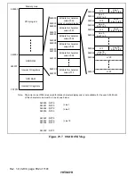
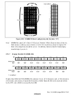
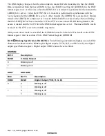
The OSD display changes when the data written to master RAM is transferred to the slave RAM.
Data is transferred from the master RAM to the slave RAM by setting the LDREQ bit in the OSD
format register to 1. At this time, when the DTMV bit is 0, transfer is performed at the moment the
LDREQ bit is set to 1; when the DTMV bit is 1, transfer is performed in synchronous with the
Vsync signal after the LDREQ bit is set to 1. After transfer, the LDREQ bit is cleared to 0. During
transfer, the LDREQ bit remains set to 1; master RAM should be accessed only after confirming
that the LDREQ bit has been cleared to 0. If the CPU accesses master RAM during transfer, the
access is invalid and the VACS bit in the OSD format register is set to 1. The master RAM can be
accessed by the CPU even in the module stop mode.
After power-down mode is cancelled, the OSDRAM must be initialized. For details on the OSD
format register, refer to section 29.6.6, OSD Format Register (DFDRM).
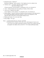
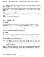
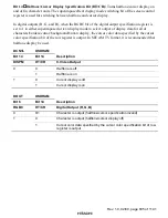
Bit 15
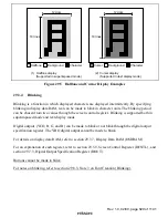
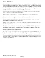
Blinking Specification Bit (BLNK): Turns blinking (intermittent display) on and off for
characters in character units. Blinking for digital outputs (YCO, R, G, and B) is set by the digital
output specification register. Digital output (YBO) cannot be set to blink.
OSDRAM
Bit 15
Description
BLNK
C.Video Output
0
Blinking is off
1
Blinking is on
DOUT
OSDRAM
Bit 4
Bit 15
Description
DOBC
BLNK
Digital Output (YCO, R, G, B)
0
Blinking is off
0
1
Blinking is off
0
Blinking is off
1
1
Blinking is on

