Rev. 1.0, 02/00, page 406 of 1141
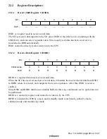
Bits 1 and 0
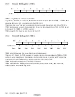
Clock Select 1 and 0 (CKS1, CKS0): These bits select the clock source for the
baud rate generator. The clock source can be selected from
φ
,
φ
/4,
φ
/16, and
φ
/64, according to
the setting of bits CKS1 and CKS0.
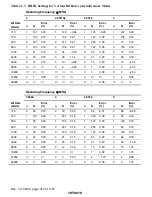
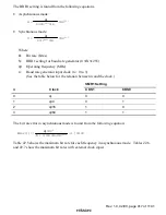
For the relation between the clock source, the bit rate register setting, and the baud rate, see
section 22.2.8, Bit Rate Register 1.
Bit 1
Bit 0
CKS1
CKS0
Description
0
φ
clock
(Initial value)
0
1
φ
/4 clock
0
φ
/16 clock
1
1
φ
/64 clock
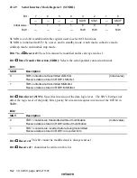
22.2.6
Serial Control Register 1 (SCR1)
7
TIE
0
R/W
6
RIE
0
R/W
5
TE
0
R/W
4
RE
0
R/W
3
MPIE
0
R/W
0
CKE0
0
R/W
2
TEIE
0
R/W
1
CKE1
0
R/W
Bit :
Initial value :
R/W :
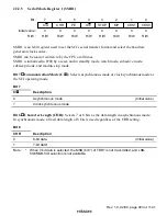
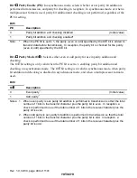
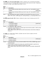
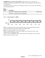
SCR1 is a register that performs enabling or disabling of SCI transfer operations, serial clock
output in asynchronous mode, and interrupt requests, and selection of the serial clock source.
SCR1 can be read or written to by the CPU at all times.
SCR1 is initialized to H'00 by a reset, and in standby mode, watch mode, subactive mode,
subsleep mode, and module stop mode.
Bit 7
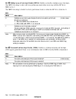
Transmit Interrupt Enable (TIE): Enables or disables transmit-data-empty interrupt
(TXI) request generation when serial transmit data is transferred from TDR1 to TSR1 and the
TDRE flag in SSR1 is set to 1.
Bit 7
TIE
Description
0
Transmit-data-empty interrupt (TXI) request disabled*
(Initial value)
1
Transmit-data-empty interrupt (TXI) request enabled
Note:
*
TXI interrupt request cancellation can be performed by reading 1 from the TDRE flag,
then clearing it to 0, or clearing the TIE bit to 0.

