Rev. 1.0, 02/00, page 400 of 1141
22.1.3
Pin Configuration
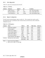
Table 22.1 shows the serial pins used by the SCI.
Table 22.1
SCI Pins
Channel
Pin Name
Symbol
I/O
Function
Serial clock pin 1
SCK1
I/O
SCI1 clock input/output
Receive data pin 1
SI1
Input
SCI1 receive data input
1
Transmit data pin 1
SO1
Output
SCI1 transmit data output
22.1.4
Register Configuration
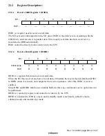
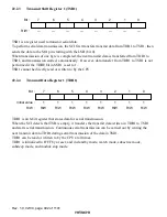
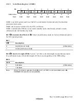
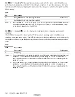
The SCI1 has the internal registers shown in table 22.2. These registers are used to specify
asynchronous mode or synchronous mode, the data format, and the bit rate, and to control the
transmitter/receiver.
Table 22.2
SCI Registers
Channel
Name
Abbrev.
R/W
Initial Value
Address
*1
Serial mode register 1
SMR1
R/W
H'00
H'D148
Bit rate register 1
BRR1
R/W
H'FF
H'D149
Serial control register 1
SCR1
R/W
H'00
H'D14A
Transmit data register 1
TDR1
R/W
H'FF
H'D14B
Serial status register 1
SSR1
R/(W)*
2
H'84
H'D14C
Receive data register 1
RDR1
R
H'00
H'D14D
1
Serial interface mode register 1
SCMR1
R/W
H'F2
H'D14E
MSTPCRH
R/W
H'FF
H'FFEC
Common
Module stop control register
MSTPCRL
R/W
H'FF
H'FFED
Notes: 1. Lower 16 bits of the address.
2. Only 0 can be written, to clear flags.

