Rev. 1.0, 02/00, page 574 of 1141
26.3.5
Operation
•
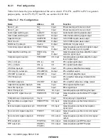
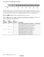
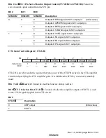
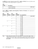
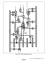
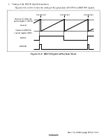
Operation of REF30 Signal Generator
The REF30 signal generator generates the reference signals required to control the phase of
the drum and capstan.
To generate the REF30 signal, set the 1/2 the reference period to the reference period
register 1 (RFD) corresponding to the 50 percent duty cycle. In playback mode, the REF30
signal is generated by free-running the REF30 signal generator. The generator has the
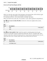
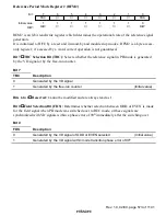
external signal synchronization function, and if the bit 4 (REX) of the reference period
mode register (RFM) is set to 1, it generates the REF30 signal from the external signal
(EXTTGR).
In record mode, the reference signal is generated from the VD signal generated in the sync
detector. Any VD drop-out caused by weak field intensity, etc., is compensated by a value
set in RFD. To cope with the VD noises, the generator automatically masks the VD for a
period about 75% of the RFD setting after REF30 signal was changed due to VD. In
record mode, the generation of the reference signal either by VD or free-run operation can
be controlled automatically using the V noise detection signal detected in the sync signal
detection circuit or manually by software. Select which is used by setting bit 6 (VNA) or 5
(CVS) of RFM.
The phase of the toggle output of the REF30 signal is cleared to L level when the mode
shifts from PB to REC (ASM). Also the frame servo function can be set, allowing for
control of the phase of REF30 signals with the field signal detected in the sync signal
detection circuit. Use bit 2 (OD/EV) of RFM for such control.
See the description of CTL mode register (CTLM) in section 26.13.5, Register Description,
as for switching over between PB, ASM and REC.
•
Operation of the Mask Circuit
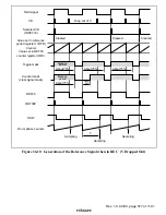
The REF30 signal generator has a toggle mask circuit and a counter mask (counter set
signal mask) circuit built-in. Each mask circuit masks irregular VD signals which may
occur when the VD signal is unstable because of weak field intensity, etc., in record mode.
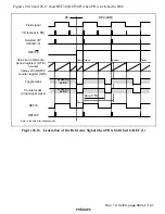
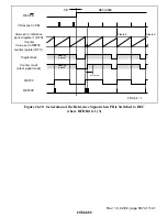
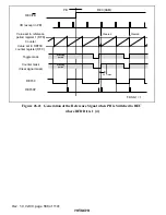
The toggle mask and counter mask circuits mask the VD automatically for about 75% of
double the period set in the reference period register 1 (RFD) after VD signal was detected
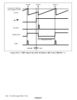
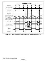
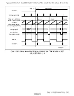
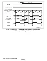
(see figure 26.9). If a VD signal dropped out and V was compensated, the toggle mask
circuit begins masking, but the counter mask circuit does not begin masking for about 25%
of the period. If VD signal was detected during such a period, the circuit does masking for
about 75% of the period after the VD detection. If not detected, it does masking for about
75% of the period after V was compensated (see figures 26.10 and 26.11).

