Rev. 1.0, 02/00, page 633 of 1141
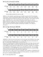
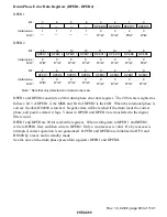
Drum Phase Error Data Registers (DPER1, DPER2)
DPER1
0
0
1
0
R*/W
2
0
R*/W
3
DPER16
DPER17
DPER18
DPER19
0
4
1
5
1
6
1
7
—
—
—
—
—
—
—
—
R*/W
R*/W
1
Bit :
Initial value :
R/W :
DPER2
8
0
9
0
R*/W
10
0
R*/W
11
DPER8
DPER9
DPER10
DPER11
0
12
0
13
0
14
0
15
DPER12
DPER13
DPER14
DPER15
R*/W
R*/W
R*/W
R*/W
R*/W
R*/W
0
Bit :
Initial value :
R/W :
Note: * Note that only detected error data can be read.
0
0
1
0
R*/W
2
0
R*/W
3
DPER0
DPER1
DPER2
DPER3
0
4
0
5
0
6
0
7
DPER4
DPER5
DPER6
DPER7
R*/W
R*/W
R*/W
R*/W
R*/W
R*/W
0
Bit :
Initial value :
R/W :
DPER1 and DPER2 constitute a 20-bit drum phase error data register. The 20 bits are weighted as
follows: bit 3 of DPER1 is the MSB, and bit 0 of DPER2 is the LSB. When the rotational phase is
correct, the data H'00000 is latched. Negative data will be latched if the drum leads the correct
phase, and positive data if it lags. Values in DPER1 and DPER 2 are transferred to the digital
filter circuit.
DPER1 and DPER are 20-bit read/write registers. When writing data to DPER 1 and DPER2,
write to DPER1 first, and then write to DPER2. Only a word access is valid. If a byte access is
attempted, correct operation is not guaranteed. DPER1 and DPER2 are initialized to H'F0 and
H'0000 by a reset, and in standby mode.
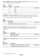
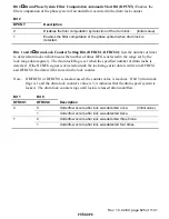
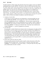
See the note on the drum phase preset data registers (DPPR1 and DPPR2).


