Rev. 1.0, 02/00, page 460 of 1141
23.1.2
Block Diagram
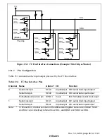
Figure 23.1 shows a block diagram of the I
2
C bus interface.
Figure 23.2 shows an example of I/O pin connections to external circuits. I/O pins are driven only
by NMOS and apparently function as NMOS open-drain outputs. However, applicable voltages to
input pins depend on the power (Vcc) voltage of this LSI.
φ
SCL
PS
Noise
canceller
Bus state
decision
circuit
Output data
control
circuit
ICCR
Clock
control
ICMR
ICSR
ICDRS
Address
comparator
Arbitration
decision
circuit
SAR, SARX
SDA
Noise
canceler
Interrupt
generator
Interrupt
request
Internal data bus
[Legend]
ICCR
ICMR
ICSR
ICDR
SAR
SARX
PS
: I
2
C control register
: I
2
C mode register
: I
2
C status register
: I
2
C data register
: Slave address register
: Slave address register X
: Prescaler
ICDRR
ICDRT
Figure 23.1 Block Diagram of I
2
C Bus Interface

