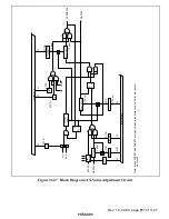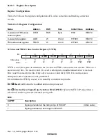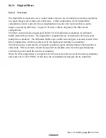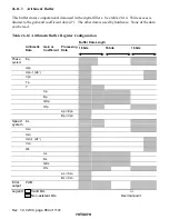
Rev. 1.0, 02/00, page 663 of 1141
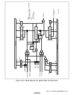
16
24
8
Z
-1
-+
*
Usn-1
GKs
+
+
Ofs
+
-
+
+
24
8
Ws
24
8
VBs
14
4
24
8
XAs
24
8
XSn
24
8
VSn
24
8
DFUout
12
24
8
α
Es
Error detector
á Add 0s to 8 bits after the decimal point
á Add the same 8-bit value as MSB
Right-bit shift of the decimal point
along with Go
PWM
Note: Go =
×
64,
×
32 are optional.
Go =
×
64,
×
32,
×
16,
×
8,
×
4,
×
2
24
8
Usn
16
DZs11 to 0
CZs11 to 0
DBs15 to 0
CBs15 to 0
16
DGKs15 to 0
CGKs15 to 0
DOfs15 to 0
COfs15 to 0
DFIC
CFIC
DFER15 to 0
CFER15 to 0
DAs15 to 0
CAs15 to 0
Bs
As
GS
KS
Go
16
Es
PWM
Digital filter
control register
Speed system
24
8
Z
-1
-+
*
1
Upn-1
GKp
+
+
OfP
+
-
24
8
Tp
24
8
VBp
24
8
XAp
24
8
VPn
24
8
Y
Phase direct test output
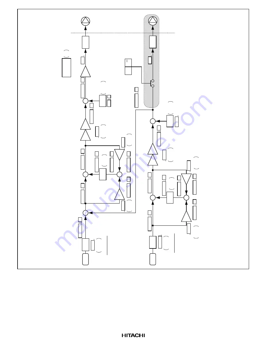
Notes 1. See figure 26.42, Z
-1
initialization circuit.
12
24
8
α
Ep
Error detector
á Add 0s to 8 bits after the decimal point
á Add the same 8-bit value as MSB
PWM
24
8
Upn
DZp11 to 0
CZp11 to 0
DBp15 to 0
CBp15 to 0
16
16
DGKp15 to 0
CGKp15 to 0
DOfp15 to 0
COfp15 to 0
DPER19 to 0
CPER19 to 0
DAp15 to 0
CAp15 to 0
BP
AP
GP
KP
20
16
16
Ep
PWM
PION
*2
á
DFUCR
á
OPTION
CP/DP
Phase system
Overflows during accumulation are ignored, and
values below the decimal point are always omitted.
2. Gain control is disabled during phase output.
Figure 26.39 Digital Filter Representation

