Rev. 1.0, 02/00, page 723 of 1141
Register Description:
•
Register configuration
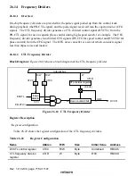
Table 26.23 shows the register configuration of the CFG frequency division circuit.
Table 26.23 Register Configuration
Name
Abbrev.
R/W
Size
Initial Value
Address
DVCFG control register
CDVC
R/W
Byte
H'60
H'D09A
CFG frequency division
register 1
CDIVR1
W
Byte
H'80
H'D09B
CFG frequency division
register 2
CDIVR2
W
Byte
H'80
H'D09C
DVCFG mask period
register
CTMR
W
Byte
H'FF
H'D09D
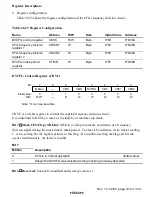
DVCFG Control Register (CDVC)
0
0
1
0
W
2
0
W
3
4
0
W
5
1
6
—
—
1
7
W
R
CMK
CMN
W
DVTRG
0
R/W*
MCGin
CRF
CPS1
CPS0
0
Note: * Only 0 can be written
Bit :
Initial value :
R/W :
CDVC is an 8-bit register to control the capstan frequency division circuit.
It is initialized to H'60 by a reset, or in stand-by or module stop mode.
Bit 7
Mask CFG Flag (MCGin): MCGin is a flag to indicate occurrence of a frequency
division signal during the mask timer's mask period. To clear it by software, write 0 after reading
1. Also, setting has the highest priority in this flag. If a condition setting the flag and 0 write
occur simultaneously, the latter is invalid.
Bit 7
MCGin
Description
0
CFG is in normal operation
(Initial value)
1
Shows that DVCFG was detected during masking (runaway detected)
Bit 6
Reserved: Cannot be modified and is always read as 1.


