Rev. 1.0, 02/00, page 139 of 1141
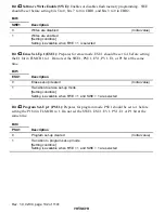
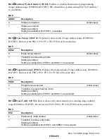
Bit 3
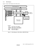
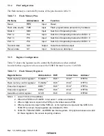
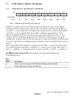
Flash Memory Control Register Enable (FLSHE): Setting the FLSHE bit to 1 enables
read/write access to the flash memory control registers. If FLSHE is cleared to 0, the flash
memory control registers are deselected. In this case, the flash memory control register contents
are retained.
Bit 3
FLSHE
Description
0
Flash memory control registers deselected
(Initial value)
1
Flash memory control registers selected
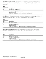
Bit 2
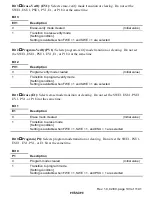
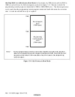
OSD ROM Enable (OSROME): Controls the OSD character data ROM (OSDROM)
access. When this bit is set to 1, the OSDROM can be accessed by the CPU, and when this bit is
cleared to 0, the OSDROM cannot be accessed by the CPU but accessed by the OSD module.
Before writing to or erasing the OSDROM in the F-ZTAT version, be sure to set this bit to 1.
Note:
During OSD display, the OSDROM cannot be accessed by the CPU. Before accessing the
OSDROM by the CPU, be sure to clear the OSDON bit in the screen control register to 0
then set the OSROME bit to 1. If the OSROME bit is set to 1 during OSD display, the
character data ROM cannot be accessed correctly by CPU.
Bit 2
OSROME
Description
0
OSD ROM is accessed by the OSD
(Initial value)
1
OSD ROM is accessed by the CPU
Bits 7, 4, 1 and 0
Reserved: Always read as 0. If 1 is written to, correct operation cannot be
guaranteed.

