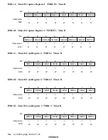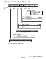
Rev. 1.0, 02/00, page 1040 of 1141
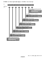
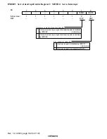
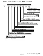
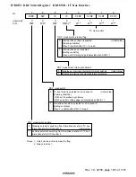
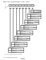
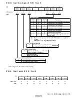
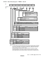
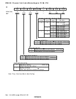
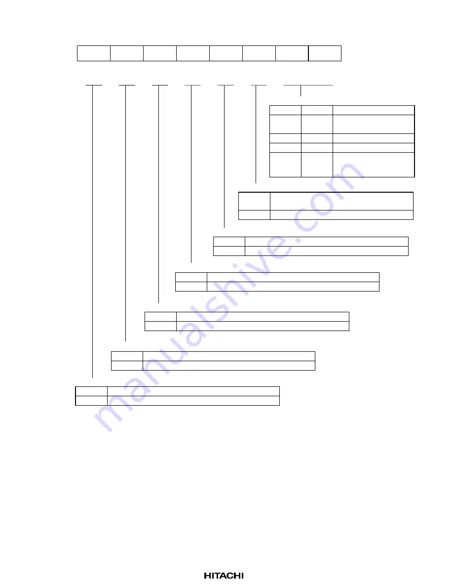
H'D106: Timer Control Register X TCRX: Timer X1
0
0
1
0
2
0
3
0
4
0
5
0
6
0
7
R/W
R/W
IEDGB
0
R/W
IEDGA
R/W
IEDGD
R/W
IEDGC
R/W
BUFEB
R/W
BUFEA
CKS0
R/W
CKS1
Capture at falling edge of input capture input A
(Initial value)
Capture at rising edge of input capture input A
0
1
Input capture edge select A
Capture at falling edge of input capture input B
(Initial value)
Capture at rising edge of input capture input B
0
1
Input capture edge select B
Capture at falling edge of input capture input C
(Initial value)
Capture at rising edge of input capture input C
0
1
Input capture edge select C
Capture at falling edge of input capture input D
(Initial value)
Capture at rising edge of input capture input D
0
1
Input capture edge select D
ICRC is not used as buffer register for ICRB
(Initial value)
ICRC is used as buffer register for ICRB
0
1
Buffer enable B
ICRC is not used as buffer register for ICRA
(Initial value)
ICRC is used as buffer register for ICRA
0
1
Buffer enable A
Clock selct bit
Clock select
0
0
CKS0
CKS1
1
0
0
1
Internal clock: count at
φ
/4
(Initial value)
Internal clock: count at
φ
/16
Internal clock: count at
φ
/64
1
1
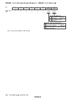
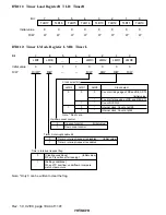
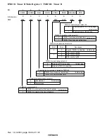
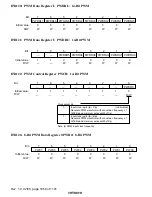
DVCFG: Edge detection
pulse selected by CFG
frequency division timer
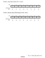
Bit
Initial value
R/W
:
:
:


