Rev. 1.0, 02/00, page 563 of 1141
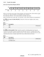
Bits 2 to 0
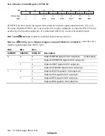
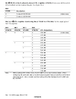
SV1 Pin Servo Monitor Output Control (SVMCR2 to SVMCR0): Select the
servo monitor signal output from the SV1 pin.
Bit 2
Bit 1
Bit 0
SVMCR2
SVMCR1
SVMCR0
Description
0
Outputs REF30 signal to SV1 output pin.
(Initial value)
0
1
Outputs CAPREF30 signal to SV1 output pin.
0
Outputs CREF signal to SV1 output pin.
0
1
1
Outputs CTLMONI signal to SV1 output pin.
0
Outputs DVCFG signal to SV1 output pin.
0
1
Outputs CFG signal to SV1 output pin.
0
Outputs DFG signal to SV1 output pin.
1
1
1
Outputs DPG signal to SV1 output pin.
CTL Gain Control Register (CTLGR)
0
0
1
0
2
0
3
0
4
0
5
6
7
—
—
—
—
CTLFB
CTLGR3
CTLGR2
CTLGR1
CTLGR0
1
1
R/W
R/W
R/W
0
CTLE/A
R/W
R/W
R/W
Bit :
Initial value :
R/W :
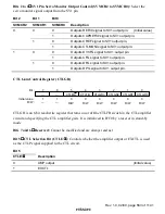
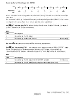
CTLGR is an 8-bit read/write register that turns on or off the CTLFB switch in the CTL amplifier
circuit and specifying the CTL amplifier gain. It is initialized to H'C0 by a reset or in stand-by
mode.
Bits 7 and 6
Reserved: Cannot be modified and are always read as 1.
Bit 5
CTL Selection Bit (CTLE/
$
$
$
$
): Controls whether the amplifier output or EXCTL is used
as the CTLP signal supplied to the CTL circuit.
Bit 5
CTLE/
$
$$
$
Description
0
AMP output
(Initial value)
1
EXCTL

