Rev. 1.0, 02/00, page 713 of 1141
26.13.9
CTL Output Section
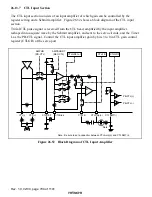
An on-chip control head amplifier is provided for writing the REC-CTL signal generated by the
write control circuit onto the tape.
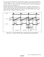
The write control circuit controls the duty cycle of the REC-CTL signal in the writing of VISS and
VASS sequences and ASM marks and the rewriting of VISS and VASS sequences. The duty
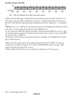
cycle of the REC-CTL signal is set in REC-CTL duty data registers 1 to 5 (RCDR1 to RCDR5).
Times calculated in terms of
φ
s (= f
OSC
/2) should be converted to appropriate data to be set in these
registers. In VISS or VASS mode, set RCDR2 for a duty cycle of 25%
±
0.5%, RCDR3 for a duty
cycle of 30%
±
0.5%, RCDR4 for a duty cycle of 57.5
±
0.5%, and RCDR5 for a duty cycle of 62.5
±
0.5%. When 1 is written in the duty I/O flag, the REC-CTL signal will be written on the tape
with a 25%
±
0.5% duty cycle when 0 is written in bit 7 (LSP7) in the bit pattern register (BTPR)
and with a 30
±
0.5% duty cycle when 1 is written. Table 26.21 shows the relationship between
the REC-CTL duty register and CTL outputs.
In ASM mark write mode, set RCDR3 for a duty cycle of 67% to 70%. An ASM mark will be
written when 0 is written in the duty I/O flag.
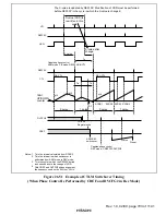
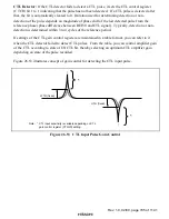
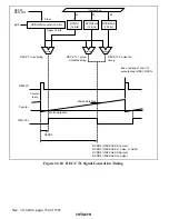
An interrupt request is generated at the rise of the reference signal after one CTL pulse has been
written. The reference signal is derived from the output signal (REF30X) of the X-value
adjustment circuit, and has a period of one frame.
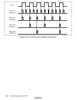
Figure 26.60 shows the timings that generate the REC-CTL signal.
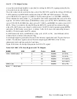
Table 26.21 REC-CTL Duty Register and CTL Outputs
MODE
D/IO
LSP7
Pulse
RCDR
Duty
0
S1
RCDR2
25
±
0.5%
0
1
L1
RCDR3
30
±
0.5%
0
S0
RCDR4
57.5
±
0.5%
VISS, VASS modes
1
1
L0
RCDR5
65.5
±
0.5%
ASM mode
0
*
RCDR3
60 to 70%
Note:
*
Don't care.

