Rev. 1.0, 02/00, page 600 of 1141
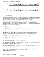
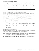
FIFO Output Pattern Register 1 (FPDRA)
8
*
9
*
W
10
*
W
11
*
12
*
W
*
W
13
14
*
15
—
—
NarrowFFA
VFFA
AFFA
VpulseA
MlevelA
1
W
W
W
ADTRGA
STRIGA
0
*
1
*
W
2
*
W
3
*
4
*
W
*
W
5
6
*
7
PPGA4
PPGA3
PPGA2
PPGA1
PPGA0
*
W
PPGA7
W
W
W
PPGA6
PPGA5
Bit :
Initial value :
R/W :
Bit :
Initial value :
R/W :
Note : * Don't care
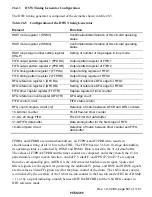
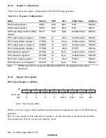
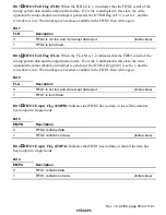
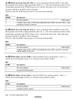
FPDRA is a buffer register for the FIFO1 output pattern register. The output pattern data written
in FPDRA is written at the same time to the position of the FIFO1 pointed by the buffer pointer.
Be sure to write the output pattern data in FPDRA before writing it in FTPRA.
FPDRA is an 16-bit write-only register. Only a word access is valid. If a byte access is
attempted, correct operation is not guaranteed. No read is valid. If a read is attempted, an
undetermined value is read out. It is not initialized by a reset, or in stand-by or module stop mode;
accordingly be sure to write data before use.
Bit 15
Reserved: Cannot be read or modified.
Bit 14
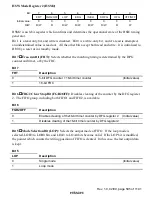
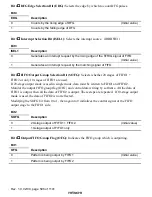
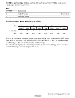
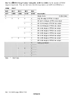
A/D Trigger A Bit (ADTRGA): Indicates a hardware trigger signal for the A/D
converter.
Bit 13
S-TRIGA Bit (STRIGA): Indicates a signal that generates an interrupt. When the
STRIGA is selected by the ISEL, modifying this bit from 0 to 1 generates an interrupt.
Bit 12
NarrowFFA Bit (NarrowFFA): Controls the narrow video head.
Bit 11
VideoFFA Bit (VFFA): Controls the video head.
Bit 10
AudioFFA Bit (AFFA): Controls the audio head.
Bit 9
VpulseA Bit (VpulseA): Used for generating an additional V signal. For details, refer to
section 26.12, Additional V Signal Generator.
Bit 8
MlevelA Bit (MlevelA): Used for generating an additional V signal. For details, refer to
section 26.12, Additional V Signal Generator.
Bits 7 to 0
PPG Output Signal A Bits (PPGA7 to PPGA0): Used for outputting a timing
control signal from port 7 (PPG).

