3.1 Installation and Connections
321
7UM62 Manual
C53000-G1176-C149-3
3.1.3.3
Switching Elements on Printed Circuit Boards
Processor Printed
Circuit Board
C–CPU–2
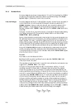
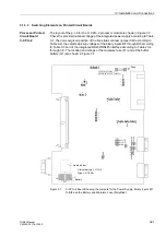
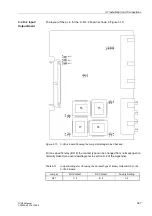
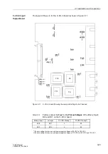
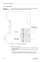
The layout of the p.c.b for the C–CPU–2 processor module is shown in Figure 3-7.
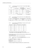
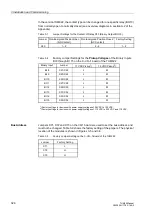
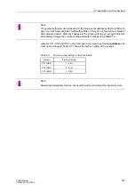
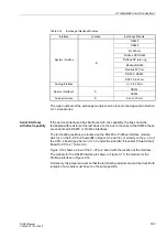
Check the provided nominal voltage of the integrated power supply according to Table
3-1, the non-energized position of the live status contact (jumper X40 according to
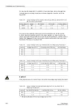
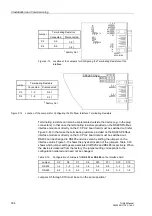
Table 3-2), the selected pickup voltages of the binary inputs BI1 through BI5 according
to Table 3-3 and of the integrated RS232/RS485 interface according to Tables 3-4
through 3-6. The location and ratings of the miniature fuse (F1) and of the buffer
battery (G1) are shown in Figure 3-7.
Figure 3-7
C-CPU–2 Board Showing the Jumpers for the Power Supply, Binary Inputs BI1
To BI5 and the Battery and Miniature Fuse (Simplified)
G1
+
–
Cable binder
Battery
X21
2
1
X51
3
1
2
X5
3
3
1
2
X52
12
34
X4
0
31
2
1
2
X55
3
4
X22
2
1
3
4
X2
3
2
1
3
4
X24
2
1
3
4
X2
5
2
1
3
4
X106
1
2
3
X104
1
2
3
X10
5
1
2
3
X
103
X
109
1
2
3
X1
07
1 2 3
X111
X110
1 2 3X108
X9
0
12
3
60-250V DC/115 V AC
T4H250V
24/48V DC
T2H250V
Lithium battery 3 V/1 Ah,
Type CR 1/2 AA
F1
Fuse

