


MPC563XM Reference Manual, Rev. 1
Freescale Semiconductor
297
Preliminary—Subject to Change Without Notice
3. Write in UT0.DSI7-0 the Syndrome Input value.
4. Select the ECC Logic Check: write a logic 1 to the UT0.EIE bit.
5. Write a logic 1 to the UT0.AIE bit to start the ECC Logic Check.
6. Wait until the UT0.AID bit goes high.
7. Compare UMISR0-4 content with the expected result.
8. Write a logic 0 to the UT0.AIE bit.
Notice that when UT0.AID is low UMISR0-4, UT1-2 and bits MRE, MRV, EIE, AIS and DSI7-0 of UT0
are not accessible: reading returns undeterminate data and write has no effect.
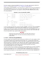
Example 11-7. ECC Logic Check
UT0
= 0xF9F99999;
/* Set UTE in UT0: Enable User Test */
UT1
= 0x55555555;
/* Set DAI31-0 in UT1: Even Word Input Data */
UT2
= 0xAAAAAAAA;
/* Set DAI63-32 in UT2: Odd Word Input Data */
UT0
= 0x803F0000;
/* Set DSI7-0 in UT0: Syndrome Input Data */
UT0
= 0x803F0008;
/* Set EIE in UT0: Select ECC Logic Check */
UT0
= 0x803F000A;
/* Set AIE in UT0: Operation Start */
do
/* Loop to wait for AID=1 */
{ tmp
= UT0;
/* Read UT0 */
} while ( !(tmp & 0x00000001) );
data0
= UMISR0;
/* Read UMISR0 content (expected 0x55555555) */
data1
= UMISR1;
/* Read UMISR1 content (expected 0xAAAAAAAA) */
data2
= UMISR2;
/* Read UMISR2 content (expected 0x55555555) */
data3
= UMISR3;
/* Read UMISR3 content (expected 0xAAAAAAAA) */
data4
= UMISR4;
/* Read UMISR4 content (expected 0x003F003F) */
UT0
= 0x00000000;
/* Reset UTE, AIE and EIE in UT0: Operation End */
11.7.12.6 Flash
Shadow Block
A Shadow block is present in the 528 Kbyte Flash macrocell.
The Shadow block can be enabled by the BIU.
When the Shadow space is enabled, all the operations are mapped to the Shadow block. User Mode
program and erase of the shadow block are enabled only when CFLASH_MCR.PEAS is high.
The Shadow block may be locked/unlocked against program or erase by using the
CFLASH_LMLR.SLOCK and CFLASH_SLLLR.SSLOCK registers.


