


MPC563XM Reference Manual, Rev. 1
1024
Freescale Semiconductor
Preliminary—Subject to Change Without Notice
NOTE:
The flush signal can be asserted along with a valid conversion result. In this case
the companion module should execute the software-reset first and then consider the
conversion result as a valid data for the filtering algorithm.
ALT_CONFIG_SEL — Alternate Configuration Selection
This field selects one of the alternate configurations according to
.
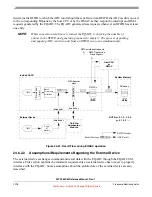
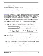
Write Configuration Command Format for On-Chip ADC Operation
describes the command message format for a write configuration command when interfacing
with the on-chip ADCs. A write configuration command is used to set the control registers of the on-chip
ADCs. No conversion data will be returned for a write configuration command. Write configuration
commands are differentiated from read configuration commands by a negated R/W bit.
Figure 24-50. Write Configuration Command Format for On-Chip ADC Operation
EOQ — End Of Queue Bit
PAUSE — Pause Bit
REP— Repeat/loop Start Point Indication Bit
EB — External Buffer Bit
BN — Buffer Number Bit
Refer to
Section , “Conversion Command Format for the Standard Configuration,”
on
.
R/W - Read/Write bit
A negated R/W indicates a write configuration command.
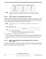
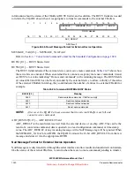
Table 24-23. Alternate Configuration Selection
ALT_CONFIG_SEL[0:7]
Alternate Configuration
0x08
1
0x09
2
0x0A
3
0x0B
4
0x0C
5
0x0D
6
0x0E
7
0x0F
8
0
1
2
3
4
5
6
7
8
9
10
11
12
13
14
15
EOQ PAU
SE
REP
RESERVE
D
EB
(0b0)
BN
R/W
(0b0)
ADC_REGISTER HIGH BYTE
CFIFO Header
ADC Command
16
17
18
19
20
21
22
23
24
25
26
27
28
29
30
31
ADC_REGISTER LOW BYTE
ADC_REG_ADDRESS
ADC Command


