


MPC563XM Reference Manual, Rev. 1
Freescale Semiconductor
1065
Preliminary—Subject to Change Without Notice
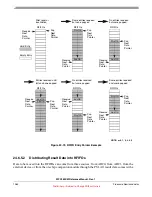
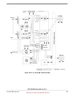
MESSAGE_TAG field and a DEST field defining what should be done with the received data. The
EQADC hardware decodes the MESSAGE_TAG and DEST fields and:
•
stores the 16-bit data into the appropriate RFIFO if the MESSAGE_TAG indicates a valid RFIFO
number, or;
•
sends the 16-bit data, the MESSAGE_TAG and the DEST data through the PSI to an on-chip
companion module (as a decimation filter), or;
•
ignores the data in case of a null or “reserved for customer use” MESSAGE_TAG.
In general received data is moved into RFIFOs as they become available, while an exception happens when
multiple results from different sources become available at the same time. In that case, result data from
ADC0 is processed first, result data from ADC1 is only process after all ADC0 data is processed, result
data from the external device is only processed after all data from ADC0/1 is processed, and finally
returned data from companion module is only processed after all data from ADC0/1 and external device
is processed.
When time-stamped results return from the on-chip ADCs, the conversion result and the time stamp are
always moved to the RFIFOs in consecutive clock cycles in order to guarantee they are always stored in
consecutive RFIFO entries.
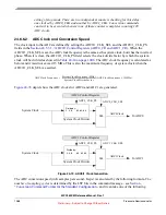
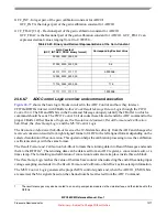
24.6.6
On-Chip ADC Configuration and Control
24.6.6.1
Enabling and Disabling the On-chip ADCs
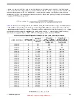
The on-chip ADCs have an enable bit (ADC0/1_EN) in the
Section 24.5.3.1, “ADC0/1 Control Registers
which allows the enabling of the ADCs only when necessary. When the
enable bit for an ADC is negated, the clock input to that ADC is stopped. The ADCs are disabled out of
reset - ADC0/1_EN bits are negated - to allow for their safe configuration. The ADC must only be
configured when its enable bit is negated. Once the enable bit of an ADC is asserted, clock input to is
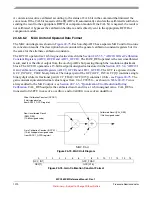
started, and the bias generator circuit is turned on. A bias generator circuit, which is common to the two
ADCs, is used to reduce the manufacturing process dependency of the ADCs and it only starts operating
when at least one of the ADCs is enabled. When the enable bits of both ADCs are negated, the bias circuit
generator is stopped.
NOTE:
Conversion commands sent to the CBuffer of a disabled ADC are ignored by the
ADC control hardware.
NOTE:
A 8ms wait time from VDDA power up to enabling ADC is required to pre-charge
the external 100nf capacitor on REFBYPC pin. This time must be guaranteed by
crystal startup time plus reset duration or user. The ADC internal bias generator
circuit will start up after 10us upon VRH/VRL and VDDA/VSSA power up and
produces a stable/required bias current to the pre-charge circuit, but the current to
other analog circuits are disabled until ADCs are enabled. As soon as the ADCs are
enabled, the bias currents to all of analog circuits will be enabled.
NOTE:
Due to legacy reasons, the EQADC will always wait 120 ADC clocks before issuing
the first conversion command following the enabling of one of on-chip ADCs, or the