


MPC563XM Reference Manual, Rev. 1
238
Freescale Semiconductor
Preliminary—Subject to Change Without Notice
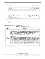
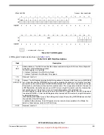
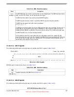
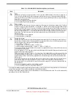
BIU4 register functions are shown in
10.3.6.13 User Multiple Input Signature Register
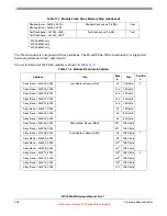
The Multiple Input Signature Register (UM0, UM1, UM2, UM3 and UM4) provides a means to evaluate
array integrity.
10.3.6.13.1
UM0 Register
The following field and bit descriptions fully define the UM0 register (
).
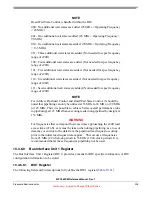
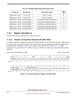
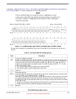
MISR register functions are shown in
Offset 0x002c
Access: User read/write
0
1
2
3
4
5
6
7
8
9
10 11 12 13 14 15 16 17 18 19 20 21 22 23 24 25 26 27 28 29 30 31
R
BIU4
W
(writability is SOC specified)
Reset
1* 1* 1* 1* 1* 1* 1* 1* 1* 1* 1* 1*
1*
1*
1*
1*
1* 1* 1* 1* 1* 1* 1* 1* 1* 1* 1* 1* 1* 1* 1* 1*
Table 10-37. BIU4 Register
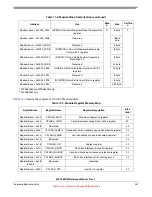
Table 10-38. BIU4 Field Descriptions
Field
Description
0-31
BIU4[31:0]
BIU4 Generic Registers. The BIU generic registers are reset based on the information stored in the
shadow block.
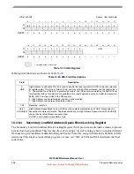
Offset 0x0048
Access: User read/write
0
1
2
3
4
5
6
7
8
9
10 11 12 13 14 15 16 17 18 19 20 21 22 23 24 25 26 27 28 29 30 31
R
MISR
W
Reset
0
0
0
0
0
0
0
0
0
0
0
0
0
0
0
0
0
0
0
0
0
0
0
0
0
0
0
0
0
0
0
0
Table 10-39. UM0 Register


