


MPC563XM Reference Manual, Rev. 1
Freescale Semiconductor
75
Preliminary—Subject to Change Without Notice
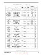
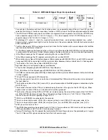
VSSE7 (x2)
I/O Ground Input
I
VSSEH7
-
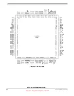
496
208
144
1
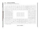
For each pin in the table, each line in the Function column is a separate function of the pin. For all I/O pins the
selection of primary pin function or secondary function or GPIO is done in the SIU except where explicitly noted.
2
The VDDE and VDDEH supply inputs are broken into segments. Each segment of slow I/O pins (VDDEH) may
have a separate supply in the 3.3 V to 5.0 V range (+/- 10%). Each segment of fast I/O (VDDE) may have a
separate supply in the 1.8 V to 3.3 V range (+/- 10%).
3
Terminology is O - output, I - input, Up - weak pull up enabled, Down - weak pull down enabled, Low - output
driven low, High - output driven high. A dash for the function in this column denotes that both the input and output
buffer are turned off.
4
Function after reset of GPI is general purpose input. A dash for the function in this column denotes that both the
input and output buffer are turned off.
5
On the 496-pin package, the Nexus function on this pin is enabled when the NEXUSCFG pin is high and Nexus
is configured to full port mode. On the 208-pin package, the Nexus function on this pin is enabled permanently.
6
In the 496-pin package, the I/O segment containing this pin is called VDDE12.
7
In the 208-pin package, the I/O segment containing this pin is called VDDE7
8
When configured as Nexus (208-pin package or 496-pin package with NEXUSCFG=1), and JCOMP is asserted
during reset, MDO[0] is driven high until the crystal oscillator becomes stable, at which time it is then negated.
9
The function of this pin is Nexus when NEXUSCFG is high.
10
High when the pin is configured to Nexus, low otherwise.
11
O/Low for the 496-package with NEXUSCFG=0; I/Up otherwise.
12
CAL_ADDR/Low for the 496-package with NEXUSCFG=0; EVTI/Up otherwise.
13
If JCOMP is asserted during reset, MDO[0] is driven high until the crystal oscillator becomes stable, at which time
it is then negated.
14
TDI and TDO are required for JTAG operation.
15
From the user point of view this is an output pad; to implement the CAN protocol this pad must also implement
the input direction.
16
The function and state of the CAN_A and eSCI_A pins after execution of the BAM program is determined by the
BOOTCFG pin.
17
The function after reset of the XTAL pin is determined by the value of the signal on the PLLCFG[1] pin. When
bypass mode is chosen XTAL has no function and should be grounded.
18
The function after reset of the EXTAL_EXTCLK pin is determined by the value of the signal on the PLLCFG[1]
pin. If the EXTCLK function is chosen, the valid operating voltage for the pin is 1.62 V to 3.6 V. If the EXTAL
function is chosen, the valid operating voltage is 3.3 V.
19
VSSPLL and VSSREG are connected to the same pin.
20
This pin is shared by two pads: VDDA_AN, using pad_vdde_hv, and VDDA_DIG, using pad_vdde_int_hv.
21
This pin is shared by two pads: VSSA_AN, using pad_vsse_hv, and VSSA_DIG, using pad_vsse_int_hv.
22
LVDS pins will not work at 3.3 V.
23
The VDDEH6 segment may be powered from 3.0 V to 5.0 V for mux address or SSI functions, but must meet the
VDDA specifications of 4.5 V to 5.25 V for analog input function.
24
If using JTAG or Nexus, the I/O segment that contains the JTAG and Nexus pins must be powered by a 5 V supply.
The 3.3 V Nexus/JTAG signals are derived from the 5 volt power supply.
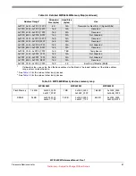
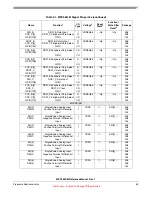
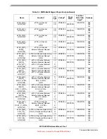
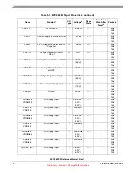
Table 3-1. MPC563xM Signal Properties (continued)
Name
Function
1
I/O
Type
Voltage
2
Reset
State
3
Function /
State After
Reset
4
Package


