


MPC563XM Reference Manual, Rev. 1
Freescale Semiconductor
253
Preliminary—Subject to Change Without Notice
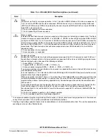
Section 11.6.2.3, “Secondary Low/Mid Address Space Block Locking Register
” for more information on CFLASH_SLMLR.
NOTE
In the event that blocks are not present (due to configuration or total
memory size), the LOCK bits defaults to locked, and are not writable. The
reset value is always 1 (independent of the shadow block), and register
writes have no effect.
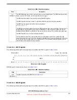
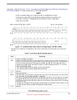
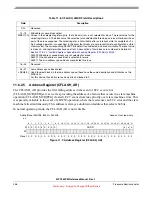
Address: Base (0xC3F8_8000) + 0x0004
Access: User read/write
0
1
2
3
4
5
6
7
8
9
10
11
12
13
14
15
R LME
0
0
0
0
0
0
0
0
0
0
SLOCK
1
1
MLOCK
W
Reset
0
0
0
0
0
0
0
0
0
0
0
1
1
1
The reset value of these bits is determined by Flash values in the shadow row. Erasing the array sets the reset
value to 1.
1
16
17
18
19
20
21
22
23
24
25
26
27
28
29
30
31
R
1
1
1
1
1
1
1
1
1
1
LLOCK
W
Reset
1
1
1
1
1
1
1
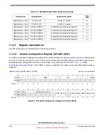
Figure 11-4. Low/Mid Address Space Block Locking Register (CFLASH_LMLR)
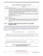
Table 11-6. CFLASH_LMLR Field Descriptions
Field
Description
0
LME
Low and mid address lock enable
Enables the locking register fields (SLOCK, MLOCK and LLOCK) to be set or cleared by register writes.
This bit is a status bit only, and cannot be written or cleared, and the reset value is 0. The method to set
this bit is to write a password, and if the password matches, the LME bit is set to reflect the status of
enabled, and is enabled until a reset operation occurs. For LME, the password 0xA1A1_1111 must be
written to the CFLASH_LMLR.
0 Low and mid address locks are disabled, and cannot be modified.
1 Low and mid address locks are enabled and can be written.
1–10
Reserved
11
SLOCK
Shadow and test lock
Locks the shadow and test sectors from programming and erase of the shadow sector only. The SLOCK
bit is not writable if a high voltage operation is suspended.
Upon reset, information from the test sector is loaded into the SLOCK bit. The SLOCK bit can be written
as a register. Reset causes the bits to go back to their test sector row value. The default value of the
SLOCK bit (assuming the corresponding shadow row bit is erased) would be locked. SLOCK is not writable
unless LME is high.
0 Shadow row is available to receive program and erase pulses; Test is available to receive program pulses
1 Shadow and Test sectors are locked for program (and shadow erase).
12–13
Reserved


