


MPC563XM Reference Manual, Rev. 1
Freescale Semiconductor
147
Preliminary—Subject to Change Without Notice
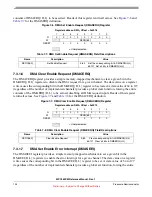
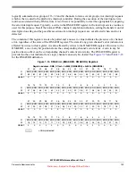
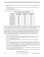
define word 6 of the TCDn structure, the dlast_sga field.
Figure 7-23. TCDn Word 6 (TCDn.dlast_sga) Field
Table 7-25. TCDn Word 6 (TCDn.dlast_sga) Field Description
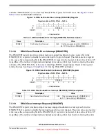
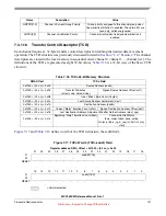
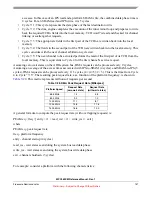
define word 7 of the TCDn structure, the biter and control/status fields.
Figure 7-24. TCDn Word 7 (TCDn.{biter,control/status}) Fields
Register address: DMA_ (32 x n) + 0x18
31
30
29
28
27
26
25
24
23
22
21
20
19
18
17
16
R
dlast_sga[31:16]
W
RESET:
-
-
-
-
-
-
-
-
-
-
-
-
-
-
-
-
15
14
13
12
11
10
9
8
7
6
5
4
3
2
1
0
R
dlast_sga[15:0]
W
RESET:
-
-
-
-
-
-
-
-
-
-
-
-
-
-
-
-
= Unimplemented
Name
Description
Value
dlast_sga[31:0]
Last destination address adjustment or
the memory address for the next transfer
control descriptor to be loaded into this
channel (scatter/gather)
if (TCD.e_sg = 0) then
Adjustment value added to the destination address at
the completion of the outer major iteration count.
This value can be applied to “restore” the destination
address to the initial value, or adjust the address to
reference the next data structure.
else
This address points to the beginning of a 0-modulo-32
region containing the next transfer control descriptor to
be loaded into this channel. This channel reload is
performed as the major iteration count completes. The
scatter/gather address must be 0-modulo-32, else a
configuration error is reported.
Register address: DMA_ (32 x n) + 0x1c
31
30
29
28
27
26
25
24
23
22
21
20
19
18
17
16
R
biter[15:0]
W
RESET:
-
-
-
-
-
-
-
-
-
-
-
-
-
-
-
-
15
14
13
12
11
10
9
8
7
6
5
4
3
2
1
0
R
bwc
major.linkch[5:0]
done active major.
e_link
e_sg
d_req int_ha
lf
int_m
aj
start
W
RESET:
-
-
-
-
-
-
-
-
0
0
-
-
-
-
-
0
= Unimplemented


