


MPC563XM Reference Manual, Rev. 1
Freescale Semiconductor
269
Preliminary—Subject to Change Without Notice
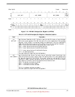
6-7
ARBM
Arbitration Mode
This 2-bit field controls the arbitration for PFLASH controllers supporting two AHB ports.
00
Fixed priority arbitration with AHB p0 > p1
01
Fixed priority arbitration with AHB p1 > p0
1-
Round-robin arbitration
This field is ignored in the <<BLOCK NAME>> implementation.
8-14
Reserved, should be cleared
15-16, 24
BK0_RWWC
Bank0 Read-While-Write Control
This 3-bit field defines the controller response to Flash reads while the array is busy with a
program (write) or erase operation.
0--
Terminate any attempted read-while-write/erase with an error response
111 Generate a bus stall for a read-while-write/erase, disable the stall notification interrupt,
disable the abort + abort notification interrupt
110 Generate a bus stall for a read-while-write/erase, enable the stall notification interrupt,
disable the abort + abort notification interrupt
101 Generate a bus stall for a read-while-write/erase, enable the operation abort, disable
the abort notification interrupt
100 Generate a bus stall for a read-while-write/erase, enable the operation abort and the abort
notification interrupt
This field is set to 0b111 by hardware reset enabling the stall-while-write/erase and disabling
the abort and notification interrupts.
17-18
B0_P1_BCFG
Bank0, Port 1 Page Buffer Configuration
This field controls the configuration of the four line buffers in the PFLASH controller. The buffers
can be organized as a “pool” of available resources, or with a fixed partition between instruction
and data buffers.
If enabled, when a buffer miss occurs, it is allocated to the least-recently-used buffer within the
group and the just-fetched entry then marked as most-recently-used. If the Flash access is for
the next-sequential line, the buffer is not marked as most-recently-used until the given address
produces a buffer hit.
00
All four buffers are available for any Flash access, that is, there is no partitioning of the
buffers based on the access type.
01
Reserved
10
The buffers are partitioned into two groups with buffers 0 and 1 allocated for instruction
fetches and buffers 2 and 3 for data accesses.
11
The buffers are partitioned into two groups with buffers 0,1,2 allocated for instruction
fetches and buffer 3 for data accesses.
This field is ignored in the <<BLOCK NAME>> implementation.
19
B0_P1_DPFE
Bank0, Port 1 Data Prefetch Enable
This field enables or disables prefetching initiated by a data read access. This field is cleared by
hardware reset.
0
No prefetching is triggered by a data read access
1
If page buffers are enabled (B0_P1_BFE = 1), prefetching is triggered by any data read
access
This field is ignored in the <<BLOCK NAME>> implementation.
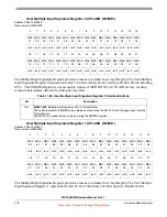
Table 11-17. PFLASH Configuration Register 2 Field Descriptions (continued)
Field
Description


