


MPC563XM Reference Manual, Rev. 1
Freescale Semiconductor
257
Preliminary—Subject to Change Without Notice
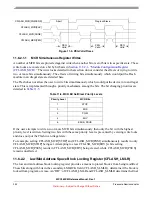
11.6.2.6
Bus Interface Unit 0 register (CFLASH_BIU0)
This register defines the configuration associated with Flash memory bank0. This typically corresponds to
the “code Flash”. It includes fields that provide specific information for up to two separate AHB ports (p0
and the optional p1). The register is described below in
and
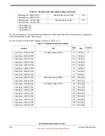
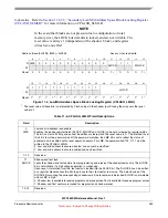
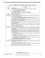
Table 11-9. CFLASH_AR Field Descriptions
Field
Description
0–8
Reserved
9–28
ADDR[3:22]
Doubleword address of first failing address in the event of an ECC error, or the address of a failure occurring
during state machine operation.
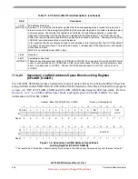
The Address Register provides the first failing address in the event of ECC error (MCR.EER set) or the first
failing address in the event of RWW error (MCR.RWE set), or the address of a failure that may have
occurred in a FPEC operation (MCR.PEG cleared). The Address Register provides also the first address
at which a ECC single error correction occurs (MCR.EDC set), if the SoC is configured to show this feature.
The ECC double error detection takes the highest priority, followed by the RWW error, the FPEC error and
the ECC single error correction. When accessed ADR will provide the address related to the first event
occurred with the highest priority. The priorities between these 4 possible events is summarized in the
following table.
This address is always a Double Word address that selects 64 bits.
In case of a simultaneous ECC Double Error Detection on both Double Words of the same page, bit AD3
will output 0. The same is valid for a simultaneous ECC Single Error Correction on both Double Words of
the same page.
In User Mode the Address Register is read only
29–31
ADDR[0:2]
Always read as 0.
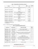
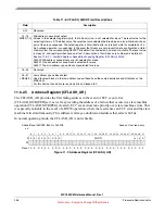
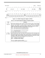
Table 11-10. ADR content: priority list
Priority Level
Error Flag
ADR content
1
MCR.EER = 1
Address of first ECC Double Error
2
MCR.RWE = 1
Address of first RWW Error
3
MCR.PEG = 0
Address of first FPEC Error
4
MCR.EDC = 1
Address of first ECC Single Error Correction


