


MPC563XM Reference Manual, Rev. 1
Freescale Semiconductor
1093
Preliminary—Subject to Change Without Notice
24.6.11.2.2
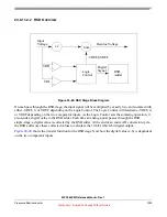
RSD Overview
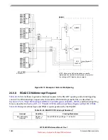
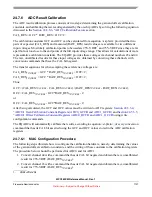
Figure 24-89. RSD Stage Block Diagram
On each pass through the RSD stage, the input signal will be multiplied by exactly two, and summed with
either -VREF, 0, or VREF, depending on the Logic Control. The Logic Control will determine -VREF, 0,
or VREF depending on the two comparator inputs. As the Logic Control sets the summing operation, it
also sends a digital value to the RSD adder. Each time an analog signal passes through the RSD
single-stage, a digital value is collected by the RSD adder. At the end of an entire AD conversion cycle,
the RSD adder uses these collected values to calculate the 12-bit/10-bit/8-bit digital output.
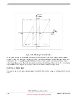
shows the transfer function for the RSD stage. Note how the digital value (a, b) is dependent
on the two comparator inputs.
x2
Sum
VRL
VRH
Input
Voltage
Logic
Control
Residue Voltage
+
-
+
-
-VREF,0,VREF
Digital
Signal
RSD
Adder


