


MPC563XM Reference Manual, Rev. 1
732
Freescale Semiconductor
Preliminary—Subject to Change Without Notice
The SCM used area is informed to the eTPU address decoding logic through the plug
etpu_scmsize_plug[4:0]. SCM unused area is decoded and returns a fixed opcode, determined by the
register ETPUSCMOFFDATAR.
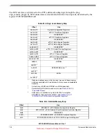
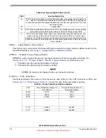
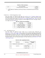
Table 23-3. High Level Memory Map
Offset
Use
0x00-0x1F
System Configuration Registers
0x20-0x2F
eTPU 1 Time Base Registers
0x30-0x3F
RESERVED
1
1
Reserved addresses must not be used. Access to these memory
positions complete with 0-wait-states, but may cause unpredictable
behavior.
0x40-0x4F
eTPU 2 Time Base Registers
0x50-0x5F
RESERVED
0x60-0x6F
eTPU 1 Extra Engine Registers
0x70-0x7F
eTPU 2 Extra Engine Registers
0x80-0x1FF
RESERVED
0x200-0x2FF
eTPU 1/2 Global Channel Registers
0x300-0x3FF
RESERVED
0x400-0x7FF
eTPU 1 Channel Registers
0x800-0xBFF
eTPU 2 Channel Registers
0xC00-0x7FFF
RESERVED
0x8000
-
0xBFFF
2
2
Actual sizes of SCM and SPRAM are MCU-dependent.
SPRAM
0xC000
-
0xFFFF
SPRAM PSE mirror
3
3
Parameter Sign Extension access area, see
”.
0x10000
-
SCM
4
4
SCM access is available only when bit VIS=1 on register
ETPUMCR, under certain conditions (see
“ETPUMCR - eTPU Module Configuration Register
”).
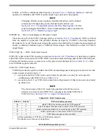
Table 23-4. Detailed Memory Map
Offset
Use
0x00
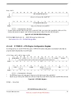
ETPUMCR - eTPU Module Configuration Register
0x04
ETPUCDCR - eTPU Coherent Dual-Parameter Controller Register
0x08
RESERVED
0x0C
ETPUMISCCMPR - eTPU MISC Compare Register
0x10
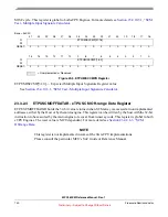
ETPUSCMOFFDATAR - eTPU SCM Off-range Data Register
1


