


MPC563XM Reference Manual, Rev. 1
510
Freescale Semiconductor
Preliminary—Subject to Change Without Notice
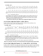
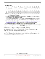
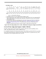
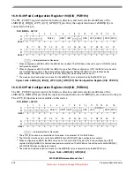
Figure 16-52. eTPU_A[24]_IRQ[12]_SCK_C_LVDS-_GPIO[138] Pad Configuration Register (SIU_PCR138)
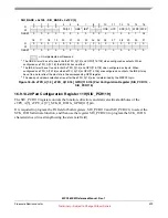
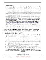
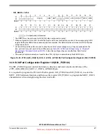
16.9.13.37 Pad Configuration Register 139 (SIU_PCR139)
The SIU_PCR139 register control the function, direction, and static electrical attributes of the
eTPU_A[25]_IRQ[13]_SCK_GPIO[139] pin.
It is required to program the PA field of both registers, SIU_PCR138 and SIU_PCR139, to select the
SCK_LVDS alternate function, and then use the register SIU_PCR139 to program the SCK_LVDS
characteristics (drive strength using the slew rate field).
SI 0x154
0
1
2
3
4
5
6
7
8
9
10
11
12
13
14
15
R
0
0
0
PA[0-2]
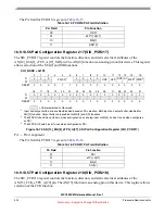
OBE
1
1
The OBE bit must be set to one for GPIO[138] when configured as output.
IBE
2
2
When configured as RQ or GPO, the IBE bit may be set to one to reflect the pin state in the corresponding GPDI
register. Setting the IBE bit to zero reduces power consumption. The IBE bit must be set to one for GPIO[138]
when configured as input.
0
0
ODE
HYS
SRC[0-1]
3
3
On the LVDS pads these bits are used to allow the control of output voltage swing. They are connected to the
lvds_opt0 and lvds_opt1 inputs of the LVDS pads (see
Table 529. “LVDS Pads Voltage Swing” in “Chapter 27
Deserial Serial Peripheral Interface (DSPI)”
). In the other pad types they assume the Slew Rate Control
functionality.
WPE
WPS
W
RESET
0
0
0
0
0
0
0
0
0
0
0
0
0
0
1
U
4
4
The weak pull up/down selection at reset for the eTPU_A[24] pin is determined by the WKPCFG pin.
16
17
18
19
20
21
22
23
24
25
26
27
28
29
30
31
R
0
0
0
0
0
0
0
0
0
0
0
0
0
0
0
0
W
RESET
0
0
0
0
0
0
0
0
0
0
0
0
0
0
0
0
= Unimplemented or Reserved


