


MPC563XM Reference Manual, Rev. 1
1176
Freescale Semiconductor
Preliminary—Subject to Change Without Notice
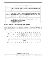
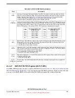
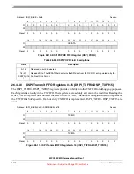
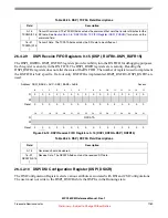
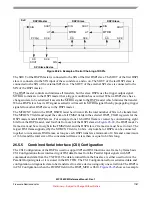
shift register of the Slave, and vice versa. At the end of a transfer, the TCF bit in the DSPI_SR is set to
indicate a completed transfer.
illustrates how Master and Slave data is exchanged.
Figure 26-19. SPI and DSI Serial Protocol Overview
The DSPI has eight Peripheral Chip Select (PCS) signals that are used to select which of the Slaves to
communicate with.
The three DSPI configurations share transfer protocol and timing properties so they are described
independently of the configuration in
Section 26.5.7, “Transfer Formats
”. The transfer rate and delay
settings are described in
Section 26.5.6, “DSPI Baud Rate and Clock Delay Generation
.”
Section 26.5.11, “Power Saving Features
,” for information on the power-saving features of the DSPI.
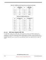
26.5.1
Modes of Operation
The DSPI has six distinct modes:
•
Master Mode
•
Slave Mode
•
Module Disable Mode
•
External Stop Mode
•
Factory Test Mode
•
Debug Mode
Master, Slave, and Module Disable Modes are block-specific mode while External Stop, Factory Test, and
Debug Modes are MCU-specific modes.
The block-specific modes are determined by bits in the DSPI_MCR. External Stop Mode, Debug Mode
and Factory Test Mode are modes that the entire MCU can enter in parallel with the DSPI being configured
in one of its block-specific modes.
26.5.1.1
Master Mode
In Master Mode the DSPI can initiate communications with peripheral devices. The DSPI operates as bus
master when the MSTR bit in the DSPI_MCR is set. The Serial Communications Clock (SCK) is
controlled by the Master DSPI. All three DSPI configurations are valid in Master Mode.
Shift Register
Baud Rate
Generator
Shift Register
SIN
SIN
SOUT
SOUT
SCK
SCK
SS
PCSx
DSPI Master
DSPI Slave


