


MPC563XM Reference Manual, Rev. 1
Freescale Semiconductor
699
Preliminary—Subject to Change Without Notice
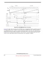
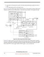
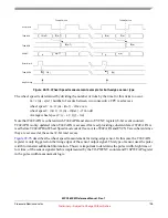
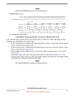
A2 is not buffered and therefore its update is immediate. If the channel is running when a change is made
this could cause either the loss of one trigger event or the generation of two trigger events within the same
period. Register A2 can be accessed by reading or writing the eMIOS200 UC Alternate A Register
(EMIOSALTA) at UC[n] base a$14.
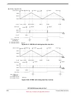
FLAG signal is set only at match on the comparator with A2. A match on the comparator with A1 or B1
or B2 has no effect on FLAG.
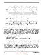
At any time, the FORCMA and FORCMB bits allow the software to force the output flip-flop to the level
corresponding to a match on A or B respectively. Any FORCMA and/or FORCMB has priority over any
simultaneous match regarding to output pin transitions. Note that the load of B2 content on B1 register at
an A match is not inhibited due to a simultaneous FORCMA/FORCMB assertion. If both FORCMA and
FORCMB are asserted simultaneously the output pin goes to the opposite of EDPOL value such as if A1
and B1 registers had the same value. FORCMA assertion causes the transfer from register B2 to B1 such
as a regular A match, regardless of FORCMB assertion.
If subsequent matches occur on comparators A1 and B, the PWM pulses continue to be generated,
regardless of the state of the FLAG bit.
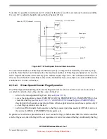
At OPWMT mode entry the output flip-flop is set to the complement of the EDPOL bit in the EMIOSC[n]
register.
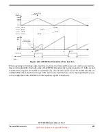
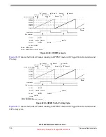
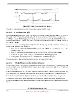
In order to achieve 0% duty cycle both registers A1 and B must be set to the same value. When a
simultaneous match on comparators A and B occur, the output flip-flop is set at every period to the
complement value of EDPOL.
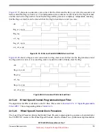
In order to achieve 100% duty cycle the register B1 must be set to a value greater than maximum value of
the selected time base. As a consequence if 100% duty cycle must be implemented the maximum counter
value for the time base is $FFFFFE for a 24-bit counter and respectively $FFFE for a 16-bit counter. When
a match on comparator A1 occurs the output flip-flop is set at every period to the value of EDPOL bit. The
transfer from register B2 to B1 is still triggered by the match at comparator A.
As with other eMIOS200 mode, the OPWMT mode will implement the Output Disable function. Setting
the ODIS bit in the eMIOS200 UC Control Register (EMIOSC[n]) will enable the Output Disable
function. If the selected Output Disable input signal is asserted for the channel, the output pin will go to
the inverse of the EDPOL. The channel will continue to operate normally, although the output will be
fixed. When the Output Disable input signal is negated, the output pin will return to operate as normal.
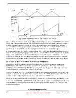
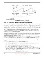
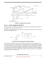
shows the Unified Channel running in OPWMT mode with Trigger Event Generation and
duty cycle update on next period update.


