


MPC563XM Reference Manual, Rev. 1
1168
Freescale Semiconductor
Preliminary—Subject to Change Without Notice
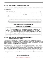
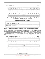
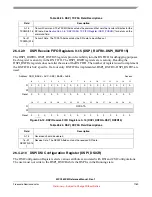
26.4.2.8
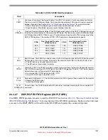
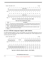
DSPI Transmit FIFO Registers 0–15 (DSPI_TXFR0–DSPI_TXFR15)
The DSPI_TXFR0 - DSPI_TXFR15 registers provide visibility into the TX FIFO for debugging purposes.
Each register is an entry in the TX FIFO. The registers are read-only and cannot be modified. Reading the
DSPI_TXFRx registers does not alter the state of the TX FIFO. The number of registers used to implement
the TX FIFO is SoC specific. If a four entry TX FIFO is implemented, DSPI_TXFR0 - DSPI_TXFR3 are
used.
Address: DSP 0x38
Access:
0
1
2
3
4
5
6
7
8
9
10
11
12
13
14
15
R
0
0
0
0
0
0
0
0
0
0
0
0
0
0
0
0
W
Reset
0
0
0
0
0
0
0
0
0
0
0
0
0
0
0
0
16
17
18
19
20
21
22
23
24
25
26
27
28
29
30
31
R
RXDATA
W
Reset
0
0
0
0
0
0
0
0
0
0
0
0
0
0
0
0
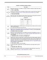
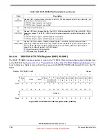
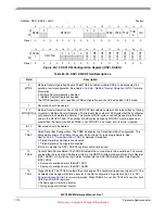
Figure 26-10. DSPI POP RX FIFO Register (DSPI_POPR)
Table 26-22. DSPI_POPR Field Descriptions
Field
Description
0–15
Reserved, should be cleared.
16–31
RXDATA[0:15
]
Received Data. The RXDATA field contains the SPI data from the RX FIFO entry pointed to by the
Pop Next Data Pointer.
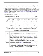
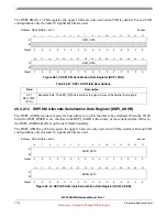
Address: DS0x3C–DS0x78
Access:
0
1
2
3
4
5
6
7
8
9
10
11
12
13
14
15
R
TXCMD
W
Reset
0
0
0
0
0
0
0
0
0
0
0
0
0
0
0
0
16
17
18
19
20
21
22
23
24
25
26
27
28
29
30
31
R
TXDATA
W
Reset
0
0
0
0
0
0
0
0
0
0
0
0
0
0
0
0
Figure 26-11. DSPI Transmit FIFO Register 0–15 (DSPI_TXFR0–DSPI_TXFR15)


