


MPC563XM Reference Manual, Rev. 1
Freescale Semiconductor
271
Preliminary—Subject to Change Without Notice
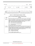
Offset 0x028
Access:
Read/write
0
1
2
3
4
5
6
7
8
9
10
11
12
13
14
15
R
BK1_APC
BK1_WWSC
BK1_RWSC
BK1_
RWW
C
W
Reset
1
1
1
1
1
1
1
1
1
1
1
1
1
1
1
1
16
17
18
19
20
21
22
23
24
25
26
27
28
29
30
31
R BK1_
RWW
C
0
0
0
0
0
0
0
BK1_
RWW
C
0
0
0
0
0
0
B1_P
0_BF
E
W
Reset
1
*
*
*
*
*
*
*
*
*
*
*
*
*
*
*
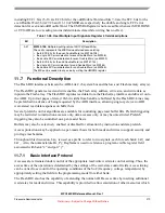
Figure 11-14. PFLASH Configuration Register 3 (PFCR3)
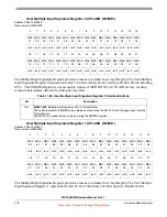
Table 11-18. PFLASH Configuration Register 3 Field Descriptions
Field
Description
0-4
BK1_APC
Bank1 Address Pipelining Control. This field is used to control the number of cycles between
Flash array access requests. This field must be set to a value appropriate to the operating
frequency of the PFLASH. The required settings are documented in the SoC specification.
Higher operating frequencies require non-zero settings for this field for proper Flash operation.
00000
Accesses may be initiated on consecutive (back-to-back) cycles
00001
Access requests require one additional hold cycle
00010
Access requests require two additional hold cycles
...
11110
Access requests require 31 additional hold cycles
11111
No address pipelining
This field is ignored in single bank Flash configurations.
5-9
BK1_WWSC
Bank1 Write Wait State Control. This field is used to control the number of wait-states to be
added to the Flash array access time for writes. This field must be set to a value appropriate to
the operating frequency of the PFLASH. The required settings are documented in the SoC
specification. Higher operating frequencies require non-zero settings for this field for proper
Flash operation. This field is set to an appropriate value by hardware reset.
00000
No additional wait-states are added
00001
1 additional wait-state is added
00010
2 additional wait-states are added
...
111111 31 additional wait-states are added
This field is ignored in single bank Flash configurations.


