


MPC563XM Reference Manual, Rev. 1
214
Freescale Semiconductor
Preliminary—Subject to Change Without Notice
10.3
Flash Memory Block (C90FL)
10.3.1
C90FL Block Overview
The primary function of the C90FL flash memory block is to serve as electrically programmable and
erasable Non-Volatile Memory (NVM). The NVM can be used for instruction and/or data storage. The
block is a non-volatile solid-state silicon memory device consisting of blocks of single-transistor storage
elements, an electrical means for selectively adding (programming) and removing (erasing) charge from
these elements, and a means of selectively sensing (reading) the charge stored in these elements. The
C90FL is addressable by word (32 bits) and page (128 bits).
The C90FL block is arranged as two functional units. The first functional unit is the C90FL Flash Core
(FC). The FC is composed of arrayed non-volatile storage elements, sense amplifiers, row selects, column
selects and charge pumps. The arrayed storage elements in the FC are subdivided into physically separate
units referred to as blocks.
The second functional unit of the C90FL is the Memory Interface (MI). The MI contains the registers and
logic which control the operation of the FC. The MI is also the interface to the PFlash Bus Interface Unit
(PFLASH_C90FL).
The PFLASH_C90FL interfaces the system bus on this device to the C90FL memory block. The PFlash
BIU is described in
Section 10.2, “Platform Flash (PFlash) Memory Controller
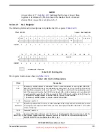
The base address for the flash bus and flash registers is 0x03F8_8000.
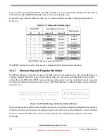
There are three address spaces:
•
Low Address Space (256 Kbytes)
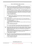
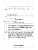
Table 10-11. PFCR2 Field Descriptions
Field
Description
Settings
LBCFG
Line Buffer Configuration - This field controls the
configuration of the four line buffers in the PFLASH
controller. The buffers can be organized as a “pool” of
available resources, or with a fixed partition between
instruction and data buffers.
In all cases, when a buffer miss occurs, it is allocated to
the least-recently-used buffer within the group and the
just-fetched entry then marked as most-recently-used.
If the flash access is for the next-sequential line, the
buffer is not marked as most-recently-used until the
given address produces a buffer hit.
This field is initialized by hardware reset to the value
contained in address 0xFF_FE00 of the shadow block
of the flash array. An erased or unprogrammed flash
sets this field to 0b11.
00
01
10
11
All four buffers are available for any flash
access, i.e., there is no partitioning of the
buffers based on the access type
Reserved
The buffers are partitioned into two groups
with buffers 0 and 1 allocated for
instruction fetches and buffers 2 and 3 for
data accesses
The buffers are partitioned into two groups
with buffers 0,1,2 allocated for instruction
fetches and buffer 3 for data accesses


