


MPC563XM Reference Manual, Rev. 1
Freescale Semiconductor
329
Preliminary—Subject to Change Without Notice
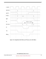
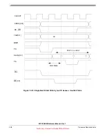
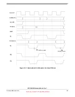
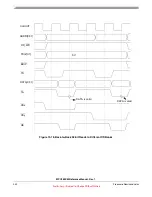
13.5.1.14 Slower-Speed Clock Modes
For memories that cannot run with a full-speed external bus, the EBI supports slower-speed clock modes.
Refer to
Section 13.2.3.5, “Slower-Speed Modes
for more details on this feature. The timing diagrams for
slower-speed modes are identical to those for full-speed mode, except that the frequency of CLKOUT is
reduced.
13.5.1.15 Stop and Module Disable Modes for Power Savings
Section 13.2.3, “Modes of Operation
for a description of the power saving modes.
13.5.1.16 Optional Automatic CLKOUT Gating
The EBI has the ability to hold the external CLKOUT pin high when the EBI’s internal master state
machine is idle and no requests are pending. The EBI outputs a signal to the pads logic in the MCU to
disable CLKOUT. This feature is disabled out of reset, and can be enabled or disabled by the ACGE bit in
the EBI_MCR.
NOTE
This feature must be disabled for multi-master systems. In those cases, one
master is getting its clock source from the other master and needs it to stay
valid continuously.
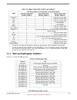
Table 13-13. Write/Byte Enable Signals Function
1
1
This table applies to aligned internal master transfers only. In the case of a misaligned internal
master transfer that is split into multiple aligned external transfers, not all of the write enables X’d
in the table will necessarily assert. See
Section 13.5.2.13, “Misaligned Access Support
Transfer
Size
TSIZ[0:1]
Address
32-Bit Port Size
16-Bit Port Size
2
2
Also applies when DBM=1 for 16-bit data bus mode.
A30
A31
WE0/
BE0
WE1/
BE1
WE2/
BE2
WE3/
BE3
WE0/
BE0
WE1/
BE1
WE2/
BE2
WE3/
BE3
Byte
01
0
0
X
X
01
0
1
X
X
01
1
0
X
X
01
1
1
X
X
16-bit
10
0
0
X
X
X
X
10
1
0
X
X
X
X
32-bit
00
0
0
X
X
X
X
X
3
3
This case consists of two 16-bit external transactions, but for both transactions the WE[0:1]/BE[0:1]
signals are the only WE/BE signals affected.
X
Burst
00
0
0
X
X
X
X
X
X


