


MPC563XM Reference Manual, Rev. 1
550
Freescale Semiconductor
Preliminary—Subject to Change Without Notice
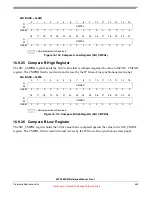
Figure 16-111. Compare B Low Register (SIU_CMPBL)
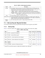
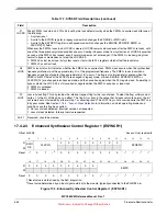
16.9.27 System Clock Register (SIU_SYSDIV)
The SIU_SYSDIV field is read/write and is reset by the IP Green-Line synchronous reset signal.
Figure 16-112. System Clock Register (SIU_SYSDIV)
SI 0x994
0
1
2
3
4
5
6
7
8
9
10
11
12
13
14
15
R
CMPBL
W
RESET
0
0
0
0
0
0
0
0
0
0
0
0
0
0
0
0
16
17
18
19
20
21
22
23
24
25
26
27
28
29
30
31
R
CMPBL
W
RESET
0
0
0
0
0
0
0
0
0
0
0
0
0
0
0
0
= Unimplemented or Reserved
SI 0x9A0
0
1
2
3
4
5
6
7
8
9
10
11
12
13
14
15
R
W
RESET
0
0
0
0
0
0
0
0
0
0
0
0
0
0
0
0
16
17
18
19
20
21
22
23
24
25
26
27
28
29
30
31
R
By-
pass
SYS-
CLKDIV[0-1
]
W
RESET
0
0
0
0
0
0
0
0
0
0
0
0
0
0
0
0
= Unimplemented or Reserved
Table 16-50. System Clock Register Field Descriptions
Field Description
0-26
Reserved
27
Bypass bit
1 = system clock divider is not bypassed
0 = system clock divider is bypassed
28-29
SYSCLKDIV[0
-1]
System Clock Divide
The SYSCLKDIV bits select the divider value for the system clock (ipg_clk). Note that the
SYSCLKDIV divider is required in addition to the RFD to allow the other sources for the system clock
(16 MHz IRC and OSC) to be divided down to slowest frequencies to improve power. The output of
the clock divider is nominally a 50% duty cycle.
00 = Divide by 2
01 = Divide by 4
10 = Divide by 8
11 = Divide by 16
30-31
Reserved


