


MPC563XM Reference Manual, Rev. 1
Freescale Semiconductor
1203
Preliminary—Subject to Change Without Notice
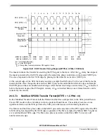
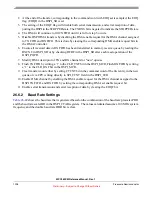
The selection bit, the start bit for a frame, is not a requirement but could be implemented by software. The
number of the frame bits can be in the range of 4 to 32 bits. In this configuration the least significant bit
of a frame should be transmitted first (LSBFE = 1).
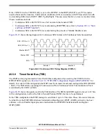
26.5.9.1
PCS Switch Over Timing
When in TSB mode it is possible to switch the set of PCS signals that are driven during the first part of the
frame to a different set of PCS signals during the second part of the frame. The bit at which this switch
over occurs is contained in the DSICR register.
In order to maximize both the setup and hold time margins on the old and new PCS signals the timing of
the switch over occurs on the active edge of the master SCK data capture between the last bit of the first
part of the frame and the first bit of the second part of the frame. For example, if the first part of the frame
is 5 bits and the second part of the frame is 10 bits the PCS signals will switch at the active edge of the
master SCK in between bits 5 and 6 of the frame as seen by the slave. The exact timing between the
external signals SCK and PCS signals will not be exactly aligned due to routing and pad differences. This
approach ensures that larger/shorter SCK periods will result in approximately symmetric
increases/decreases of setup and hold margins on the PCS signals. The setup time for the PCS signals
before the first bit of the first part of the frame and the hold time for the PCS signals after the last bit of
the second part of the frame are unchanged in this mode with respect to the other modes and remain
controlled by the CSC and ASC delay fields respectively when not in Continuous SCK mode.
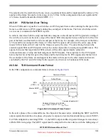
26.5.9.2
TSB Command Frame Format
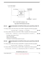
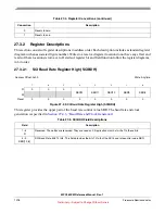
In the TSB configuration a command frame is shown in
.
Figure 26-40. Command Frame Format
In the active phase of the command frame, the chip select becomes active validating the SOUT and SCK
output signals. Outside the active phase, chip select is at passive level and invalid data may occur at SOUT.
For TSB configuration, assuming CPOL = 0, the SOUT output and the chip select changes its state always
with the SCK rising edge. The SOUT signal must be sampled in the slave device with the falling edge of
SCK
PCS
Master SOUT
Invalid
Command Frame
t
DT
Command Frame = 0 to 32 bits
LSB
1
Command Selection Bit
(CPOL = 0)
Active Phase
t
DT
= from 1 to (PDT * DT / f
sys
)T
SCK


