


MPC563XM Reference Manual, Rev. 1
1342
Freescale Semiconductor
Preliminary—Subject to Change Without Notice
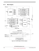
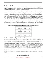
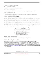
The regulator is powered by VDDREG and works in the range 4.0V to 5.5V, down to 4.0V with lower
current drive capabilities, and uses the bandgap voltage as absolute reference. The 3.3V regulator output
is connected to an I/O pad (VDD3p3) for external capacitance decoupling, then all blocks (except the
Flash) that need a 3.3V supply will be connected to the VDD3p3 pad. The 3.3V Flash power supply is
taken at a pad next to the regulator I/O, which will be double bonded together with the VDD3p3 pad. In
this way it is possible to have probe test with independent Flash 3V supply.
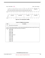
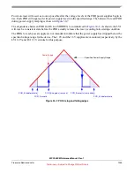
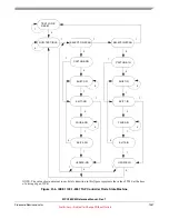
Figure 30-6. Vreg 3.3V power connection
Tolerance of the 3.3V supply is +/-6% including line and load variation. The regulator output voltage is
adjustable via software by writing to the V33TRIM field of the TRIMR register, which selects one of the
16 voltages available through the appropriate tapped output of a 24-leg resistor chain centered in 3.39V.
The taps are set between 3.15V and 3.60V at 30mV intervals. Metal options are available to map the 16
selection points onto any of the 24 resistors, in any arrangement, giving a minimum resolution of 30 mV.
The reset value of the 4-bit register is “0000”, corresponding to nominal voltage of 3.39V.
The 3.3V supply can be connected internally, on die, to a 5V ADC channel such that the actual voltage
may be read.
The output of the 3.3V regulator can be increased by +20% to stress the 3.3V logic test during burn-in
(HTOL test). For more details, please refer to the pmc Test Guide.
Osc
Vreg 3.3
Vref_3p3
Vreg 1.2
Internal 3.3V
Supply
VDD3p3
Flash
VDDREG
VDDREG


