


MPC563XM Reference Manual, Rev. 1
Freescale Semiconductor
1013
Preliminary—Subject to Change Without Notice
FMTA — Conversion Data Format for Alternate Configuration
If the DEST field is not 0b000, the FMTA bit specifies how the 12-bit conversion data returned by the
ADCs is formatted into the 16-bit data which is sent to the parallel side interface. The same applies
from the data that returns from the side interface to be stored in the RFIFOs.
1 = Right justified signed
0 = Right justified unsigned
RESSEL[0:1] — ADC Resolution Selection
The RESSEL[0:1] field selects the resolution of the ADC according to
PRE_GAIN[0:1] — ADC Pre-gain control
The PRE_GAIN[0:1] controls the gain of the ADC input stage by changing the internal ADC iterations
in the gain stage. The gain is selected according to
24.5.3.7
ADC0/1 Alternate Gain Registers (ADC0_AGR1-2 and ADC1_AGR1-2)
The Alternate Gain Registers (ADC0_AGRx and ADC1_AGRx, x=1-2) contain the gain calibration
constants used to fine-tune the ADCs conversion results for alternate configurations 1 or 2. A conversion
from an ADC uses the corresponding ADC0_AGRx or ADC1_AGRx register when the conversion
command (with the alternate configuration format) is written to an address in the range 0x08-0x09 of the
on-chip ADC memory map. Refer to
Section 24.6.6.6, “ADC Calibration Feature
for details about the
calibration scheme used in the EQADC.
Table 24-17. Resolution Selection
RESSEL[0:1]
Definition
00
ADC set to 12-bits resolution
01
ADC set to 10-bits resolution
10
ADC set to 8-bits resolution
11
Reserved
Table 24-18. ADC Pre-Gain Control Bits
Pre_gain[0:1]
Description
00
X1 gain
01
X2 gain
10
X4 gain
11
Reserved
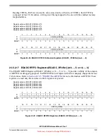
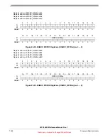
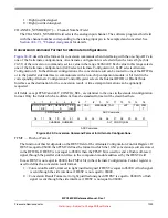
ADC0 Register address: 0x31
ADC0 Register address: 0x35
0
1
2
3
4
5
6
7
8
9
10
11
12
13
14
15
R
0
ALTGCC0x
W
RESET:
0
0
0
0
0
0
0
0
0
0
0
1
1
1
1
1
= Unimplemented or Reserved
Figure 24-43. ADC0/1 Alternate x Gain Register (ADC0/1_AGRx, x=1-2)


