


MPC563XM Reference Manual, Rev. 1
718
Freescale Semiconductor
Preliminary—Subject to Change Without Notice
23.1.1
Overview
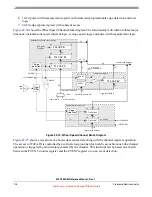
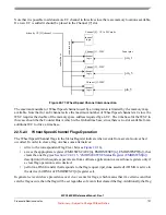
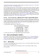
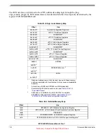
shows a top-level eTPU block diagram. It displays a dual eTPU Engine configuration,
although a single eTPU Engine configuration is also possible.
Figure 23-1. eTPU Block Diagram
eTPU Engine
is responsible for processing input pin transitions and output pin waveform generation
based on the
Time Bases
. Each eTPU Engine has its own microprocessor and dedicated hardware for
processing signals on I/O pins and can also interface with external time bases through the Red Line Bus.
Both eTPU Engine CPUs, hereafter called
microengines
, fetch microinstructions from a
Shared Code
Memory - SCM
.
Shared Parameter RAM
-
SPRAM -
holds eTPU application parameters and work data. It is accessed
by Host and both microengines.
PINS
eTPU Engine 2
eTPU Engine 1
SHARED
P.RAM
IPI SkyBlue, Green, Indigo, DarkBlue lines
SHARED CODE MEMORY
SHARED
BIU
REGISTERS
REGISTERS
SCM
PINS
HOST CPU
Red Line
Red Line
Debug If
Debug If
IPI
Purple
IPI
Purple