


MPC563XM Reference Manual, Rev. 1
Freescale Semiconductor
321
Preliminary—Subject to Change Without Notice
13.4.1.4
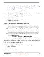
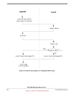
EBI Base Registers (EBI_BR0-EBI_BR3, EBI_CAL_BR0-3)
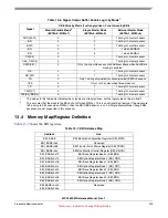
Figure 13-5. EBI Base Registers (EBI_BR0-EBI_BR3, EBI_CAL_BR0-3)
The EBI Base Registers are used to define the base address and other attributes for the corresponding chip
select.
BA — Base Address
These bits are compared to the corresponding unmasked address signals among ADDR[0:16] of the
internal address bus to determine if a memory bank controlled by the memory controller is being
accessed by an internal bus master.
NOTE
An MCU may have some of the upper bits of the BA field tied to a fixed
value internally in order to restrict the address range of the EBI for that
MCU. Refer to the device-specific SoC Guide to see which bits are tied off,
if any, for a particular MCU. Tied-off bits can be read but not written. These
bits are ignored by the EBI during the chip-select address comparison.
However, the internal bridge of the MCU most likely requires that the
chip-select banks be located in memory regions corresponding to the fixed
values chosen.
PS — Port Size
The PS bit determines the data bus width of transactions to this chip-select bank.
NOTE
In the case where the DBM bit in EBI_MCR is set for 16-bit Data Bus
Mode, the PS bit value is ignored and is always treated as a ’1’ (16-bit port).
1 = 16-bit port
0 = 32-bit port
AD_MUX — Address on Data Bus Multiplexing
E0x10, E0x18, E0x20, E0x28,
E0x40, E0x48, E0x50, E0x58
0
1
2
3
4
5
6
7
8
9
10
11
12
13
14
15
R
BA
W
RESET:
1
1
Some upper bits of the BA field may be tied to a fixed value, in which case the reset value is this fixed value and not zero.
Refer to the device-specific SoC Guide to see which bits this applies to, if any.
0
0
0
0
0
0
0
0
0
0
0
0
0
0
0
0
16
17
18
19
20
21
22
23
24
25
26
27
28
29
30
31
R
BA
0
0
0
PS
0
0
0
AD_
MUX
BL
WEB
S
TBDI
P
0
SETA
BI
V
W
RESET:
0
0
0
0
0
0
0
0
0
0
0
0
0
0
1
0
= Unimplemented or Reserved