


MPC563XM Reference Manual, Rev. 1
Freescale Semiconductor
1325
Preliminary—Subject to Change Without Notice
29.6
Functional Description
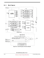
29.6.1
General
This section gives detailed information on the internal operation of the module. Each timer can be used to
generate trigger pulses as well as to generate interrupts, each interrupt will be available on a separate
interrupt line. Additionally the RTI timer can be used to wakeup the processor.
29.6.1.1
Timers / RTI
The timers generate triggers at periodic intervals, when enabled. They load their start values, as specified
in their LDVAL registers, then count down until they reach 0. Then they load their respective start value
again. Each time a timer reaches 0, it will generate a trigger pulse, and set the interrupt flag.
All interrupts can be enabled or masked (by setting the TIE bits in the TCTRL registers). A new interrupt
can be generated only after the previous one is cleared. Since in the case of the RTI, clearing the interrupt
crosses clock domains, a minimum load value of 32 should be maintained.
If desired, the current counter value of the timer can be read via the CVAL registers. The value of the RTI
counter can be delayed considerably, as it is synchronized to the bus clock from the RTI clock domain.
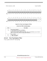
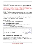
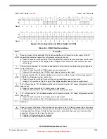
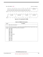
Offset channe 0x0C
Access: Read/Write
0
1
2
3
4
5
6
7
8
9
10
11
12
13
14
15
R
0
0
0
0
0
0
0
0
0
0
0
0
0
0
0
0
W
Reset
0
0
0
0
0
0
0
0
0
0
0
0
0
0
0
0
16
17
18
19
20
21
22
23
24
25
26
27
28
29
30
31
R
0
0
0
0
0
0
0
0
0
0
0
0
0
0
0
TIF
W
Reset
0
0
0
0
0
0
0
0
0
0
0
0
0
0
0
0
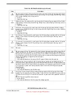
Figure 29-6. Timer Flag Register (TFLG)
Table 29-7. TFLG Field Descriptions
Field
Description
TIF
Time Interrupt Flag. TIF is set to 1 at the end of the timer period.This flag can be cleared only by
writing it with a 1. Writing a 0 has no effect. If enabled (TIE = 1), TIF causes an interrupt request.
0 Time-out has not yet occurred
1 Time-out has occurred


