


MPC563XM Reference Manual, Rev. 1
1152
Freescale Semiconductor
Preliminary—Subject to Change Without Notice
26.3.2.8
SCK — Serial Clock
SCK is a serial communication clock signal. In Master Mode, the DSPI generates the SCK. In Slave Mode,
SCK is an input from an external bus master.
26.3.2.9
HT — Hardware Trigger
HT is a trigger input signal that is used with Multiple Transfer Operations in DSI Configuration.
In Master Mode while in DSI or CSI Configurations, the HT signal initiates a data transfer when the TRRE
bit in the DSPI_DSICR is set and a rising or falling edge is detected on HT. Which edge to trigger on is
determined by the TPOL bit in the DSPI_DSICR.
In Slave Mode, the DSPI generates a trigger pulse on the MTRIG pin when a rising or falling edge is
detected on HT. Which edge that generates an output pulse is selected by the TPOL bit in the
DSPI_DSICR.
26.4
Memory Map and Register Definition
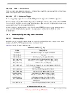
26.4.1
Memory Map
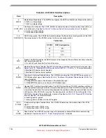
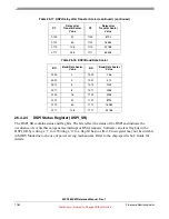
Register accesses to memory addresses that are reserved or undefined result in a transfer error. Write
access to the DSPI_POPR register also result in a transfer error.
shows the DSPI memory map.
Table 26-3. DSPI Memory Map
Address
Register Name
DSPI_BASE
DSPI Module Configuration Register (DSPI_MCR)
DS0x4
Reserved
DS0x8
DSPI Transfer Count Register (DSPI_TCR)
DS0xC–
DS0x28
DSPI Clock and Transfer Attributes Register 0 (DSPI_CTAR0) -
DSPI Clock and Transfer Attributes Register 7 (DSPI_CTAR7)
1
DS0x2C
DSPI Status Register (DSPI_SR)
DS0x30
DSPI DMA/Interrupt Request Select and Enable Register (DSPI_RSER)
FIFO Registers
DS0x34
DSPI Push TX FIFO Register (DSPI_PUSHR)
DS0x38
DSPI Pop RX FIFO Register (DSPI_POPR)
DS0x3C -
DS0x78
DSPI Transmit FIFO Register 0 (DSPI_TXFR0) -
DSPI Transmit FIFO Register 15 (DSPI_TXFR15)
2
DS0x7C -
DS0xB8
DSPI Receive FIFO Register 0 (DSPI_RXFR0) -
DSPI Receive FIFO Register 15 (DSPI_RXFR15)
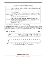
DSI Registers
DS0xBC
DSPI DSI Configuration Register (DSPI_DSICR)


