


MPC563XM Reference Manual, Rev. 1
Freescale Semiconductor
275
Preliminary—Subject to Change Without Notice
The User Test 1 Register allows to enable the checks on the ECC logic related to the 32 LSB of the Double
Word. The User Test 1 Register is not accessible whenever MCR.DONE or UT0.AID are low: reading
returns indeterminate data while writing has no effect.
User Test 2 register (CFLASH_UT2)
Address Offset: 0x00044
Reset value: 0x00000000
The User Test 2 Register allows to enable the checks on the ECC logic related to the 32 MSB of the Double
Word. The User Test 2 Register is not accessible whenever MCR.DONE or UT0.AID are low: reading
returns indeterminate data while writing has no effect.
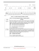
16
17
18
19
20
21
22
23
24
25
26
27
28
29
30
31
DAI1
5
DAI1
4
DAI1
3
DAI1
2
DAI1
1
DAI1
0
DAI0
9
DAI0
8
DAI0
7
DAI0
6
DAI0
5
DAI0
4
DAI0
3
DAI0
2
DAI0
1
DAI0
0
rw/0
rw/0
rw/0
rw/0
rw/0
rw/0
rw/0
rw/0
rw/0
rw/0
rw/0
rw/0
rw/0
rw/0
rw/0
rw/0
Table 11-20. User Test 1 register field descriptions
Bit
Description
0-31
DAI31-00
:
Data Array Input 31-0
(Read/Write)
These bits represents the input of even word of ECC logic used in the ECC Logic Check. The DAI31-00
correspond to the 32 array bits representing Word 0 within the double word.
0: The array bit is forced at 0.
1: The array bit is forced at 1.
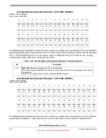
0
1
2
3
4
5
6
7
8
9
10
11
12
13
14
15
DAI6
3
DAI6
2
DAI6
1
DAI6
0
DAI5
9
DAI5
8
DAI5
7
DAI5
6
DAI5
5
DAI5
4
DAI5
3
DAI5
2
DAI5
1
DAI5
0
DAI4
9
DAI4
8
rw/0
rw/0
rw/0
rw/0
rw/0
rw/0
rw/0
rw/0
rw/0
rw/0
rw/0
rw/0
rw/0
rw/0
rw/0
rw/0
16
17
18
19
20
21
22
23
24
25
26
27
28
29
30
31
DAI4
7
DAI4
6
DAI4
5
DAI4
4
DAI4
3
DAI4
2
DAI4
1
DAI4
0
DAI3
9
DAI3
8
DAI3
7
DAI3
6
DAI3
5
DAI3
4
DAI3
3
DAI3
2
rw/0
rw/0
rw/0
rw/0
rw/0
rw/0
rw/0
rw/0
rw/0
rw/0
rw/0
rw/0
rw/0
rw/0
rw/0
rw/0
Table 11-21. User Test 2 register field descriptions
Bit
Description
0-31
DAI63-32
:
Data Array Input 63-32
(Read/Write)
These bits represents the input of odd word of ECC logic used in the ECC Logic Check. The DAI63-32
correspond to the 32 array bits representing Word 1 within the double word.
0: The array bit is forced at 0.
1: The array bit is forced at 1.


