


MPC563XM Reference Manual, Rev. 1
1230
Freescale Semiconductor
Preliminary—Subject to Change Without Notice
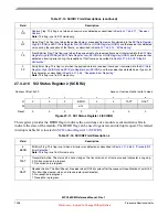
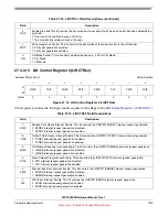
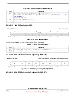
27.3.2.15 LIN Control Register 3 (LINCTRL3)
This register provides the interrupt enable signals for the flags in the
LIN Status Register 2 (LINSTAT2)
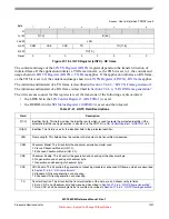
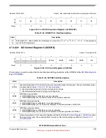
27.3.2.16 LIN TX Register (LINTX)
1
CKIE
Checksum Error Interrupt Enable. This bit controls the LINSTAT1[CKERR] interrupt request generation.
0 CKERR interrupt request generation disabled.
1 CKERR interrupt request generation enabled.
0
FCIE
Frame Complete Interrupt Enable. This bit controls the LINSTAT1[FRC] interrupt request generation.
0 FRC interrupt request generation disabled.
1 FRC interrupt request generation enabled.
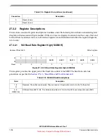
Address Offset: 0x0E
Write: Anytime
7
6
5
4
3
2
1
0
R
0
0
0
0
0
0
UQIE
OFIE
W
Reset
0
0
0
0
0
0
0
0
Figure 27-16. LIN Control Register 3 (LINCTRL3)
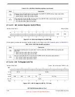
Table 27-20. LINCTRL3 Field Descriptions
Field
Description
1
UQIE
Unrequested Data Received Interrupt Enable. This bit controls the LINSTAT2[UREQ] interrupt request
generation.
0 UREQ interrupt request generation disabled.
1 UREQ interrupt request generation enabled.
0
OFIE
Overflow Interrupt Enable. This bit controls the LINSTAT2[OVFL] interrupt request generation.
0 OVFL interrupt request generation disabled.
1 OVFL interrupt request generation enabled.
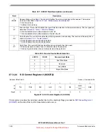
Address Offset: 0x10
Access: User write (when TXRDY is set)
Byte
7
6
5
4
3
2
1
0
R
1st W
P[1:0]
ID[5:0]
2nd W
LEN
3rd W
CSM
CSE
CRC
TD
TO[11:8]
4th+ W
DATA
Reset
0
0
0
0
0
0
0
0
Figure 27-17. LIN TX Register (LINTX) - TX Frame
Table 27-19. LINCTRL2 Field Descriptions (continued)
Field
Description


