


MPC563XM Reference Manual, Rev. 1
Freescale Semiconductor
473
Preliminary—Subject to Change Without Notice
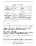
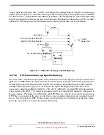
Figure 16-4. SIU External Interrupt Input Multiplexing
16.7.5.3
Multiplexed Inputs for DSPI Multiple Transfer Operation
To support multiple DSPIs transfer operations, an input multiplexor is required for the SIN, SS, SCK IN,
and Trigger signals of each DSPI. These DSPIs input sources can be a pin or respectively the SOUT,
PCS[0], SCK OUT, PCSS of any other DSPI. They are individually specified in the DSPI Input Select
Register (SIU_DISR).
Section 26.5.4.6, “Multiple Transfer Operation (MTO),”
for more information on Multiple Transfer
Operation.
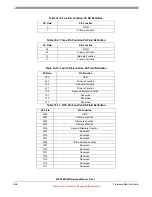
16.8
Memory Map
is the address map for the SIU registers.
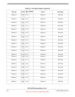
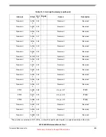
Table 16-2. SIU Address Map
Address
Use
Register size
(bits)
SIU_BASE
MCU ID Register 2 (SIU_MIDR2)
32
SI 0x4
MCU ID Register (SIU_MIDR)
32
SI 0x8
SIU Test Register (SIU_TST)
32
SI 0xC
Reset Status Register (SIU_RSR)
32
SI 0x10
System Reset Control Register (SIU_SRCR)
32
SI 0x14
SIU External Interrupt Status Register (SIU_EISR)
32
SI 0x18
DMA/Interrupt Request Enable Register (SIU_DIRER)
32
SI 0x1C
DMA/Interrupt Request Select Register (SIU_DIRSR)
32
SI 0x20
Overrun Status Register (SIU_OSR)
32
SI 0x24
Overrun Request Enable Register (SIU_ORER)
32
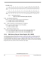
D
Q
flip-flop
C
D
Q
flip-flop
C
SIU_EIISR[0:1]
DSPI_B[0] Serialized Output
DSPI_C[1] Serialized Output
1b0
IRQ[0]
eMIOS[14]_IRQ[0]_eTPU_A[29]_GPIO[193]