


MPC563XM Reference Manual, Rev. 1
634
Freescale Semiconductor
Preliminary—Subject to Change Without Notice
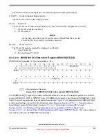
22.4.2.3
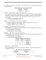
eMIOS200 Output Update Disable (EMIOSOUDIS)
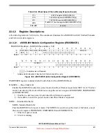
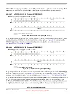
EMIOSOUDIS address: eMIOS200 base a$08
Figure 22-4. eMIOS200 Output Update Disable Register (EMIOSOUDIS)
OU[n] — Channel [n] Output Update Disable bit
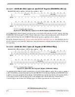
When running MC, MCB or an output mode, values are written to registers A2 and B2. OU[n] bits are
used to disable transfers from registers A2 to A1 and B2 to B1. Each bit controls one channel.
1 = Transfers disabled
0 = Transfer enabled. Depending on the operation mode, transfer may occur immediately or in the
next period. Unless stated otherwise, transfer occurs immediately.
The OU bit for Wheel Speed Channel is reserved and reads 0.
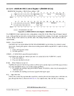
22.4.2.4
eMIOS200 Disable Channel (EMIOSUCDIS)
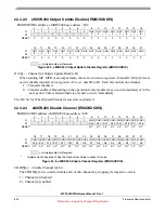
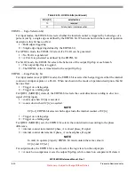
EMIOSUCDIS address: eMIOS200 base a$0C
Figure 22-5. eMIOS200 Enable Channel Register (EMIOSUCDIS)
CHDIS[n] — Enable Channel [n] bit
The CHDIS[n] bit is used to disable each of the channels by stopping its respective clock.
1 = Channel [n] disabled
0 = Channel [n] enabled
0
1
2
3
4
5
6
7
8
9
10
11
12
13
14
15
R
0
0
0
0
0
0
0
0
OU2
3
OU2
2
OU2
1
OU2
0
OU1
9
OU1
8
OU1
7
OU1
6
W
RESET:
0
0
0
0
0
0
0
0
0
0
0
0
0
0
0
0
16
17
18
19
20
21
22
23
24
25
26
27
28
29
30
31
R
OU1
5
OU1
4
OU1
3
OU1
2
OU1
1
OU1
0
OU9 OU8 OU7 OU6 OU5 OU4 OU3 OU2 OU1 OU0
W
RESET:
0
0
0
0
0
0
0
0
0
0
0
0
0
0
0
0
= Unimplemented or Reserved
0
1
2
3
4
5
6
7
8
9
10
11
12
13
14
15
R
0
0
0
0
0
0
0
0
CHDI
S23
CHDI
S22
CHDI
S21
CHDI
S20
CHDI
S19
CHDI
S18
CHDI
S17
CHDI
S16
W
RESET:
0/1
1
1
Implementation dependent. See the Device User Guide to check this value
0/1
1
0/1
1
0/1
1
0/1
1
0/1
1
0/1
1
0/1
1
16
17
18
19
20
21
22
23
24
25
26
27
28
29
30
31
R
CHDI
S15
CHDI
S14
CHDI
S13
CHDI
S12
CHDI
S11
CHDI
S10
CHDI
S9
CHDI
S8
CHDI
S7
CHDI
S6
CHDI
S5
CHDI
S4
CHDI
S3
CHDI
S2
CHDI
S1
CHDI
S0
W
RESET:
0/1
1
0/1
1
0/1
1
0/1
1
0/1
1
0/1
1
0/1
1
0/1
1
0/1
1
0/1
1
0/1
1
0/1
1
0/1
1
0/1
1
0/1
1
0/1
1
= Unimplemented or Reserved