


MPC563XM Reference Manual, Rev. 1
680
Freescale Semiconductor
Preliminary—Subject to Change Without Notice
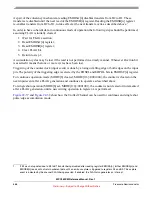
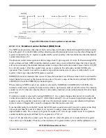
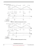
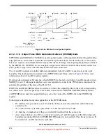
deasserted which is indicated by the A1 match negedge detection signal. If register A1 is set to $4 the
output pin transitions 4 counter periods after the cycle had started, plus one system clock cycle. Note that
in the example shown in
the internal counter prescaler has a ratio of two.
Figure 22-52. OPWFMB A1 and B1 match to Output Register Delay
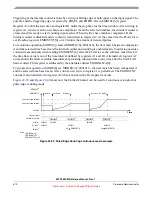
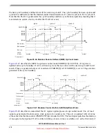
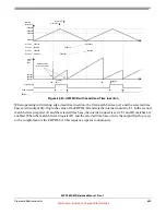
describes the generated output signal if A1 is set to $0. Since the counter does not reach zero
in this mode, the channel internal logic infers a match as if A1=$1 with the difference that in this case, the
posedge of the match signal is used to trigger the output pin transition instead of the negedge used when
A1=$1. Note that A1 posedge match signal from cycle
n+1
occurs at the same time as B1 negedge match
signal from cycle
n
. This allows to use the A1 posedge match to mask the B1 negedge match when they
occur at the same time. The result is that no transition occurs on the output flip-flop and a 0% duty cycle
is generated.
8
1
4
match A1 negedge detection
5
A1 value
$000004
A1 match
A1 match negedge detection
output pin
EDPOL = 0
EMIOSCNT
TIME
match B1 negedge detection
B1 match
B1 match negedge detection
B1 value
$000008
system clock
prescaler
Prescaler ratio = 2


