


MPC563XM Reference Manual, Rev. 1
Freescale Semiconductor
681
Preliminary—Subject to Change Without Notice
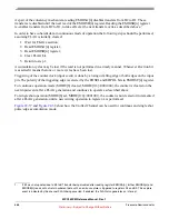
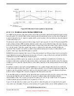
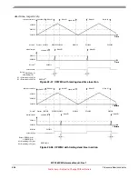
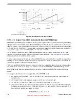
Figure 22-53. OPWFMB Mode with A1 = 0 (0% duty cycle)
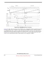
describes the timing for the A1 and B1 registers load. The A1 and B1 load use the same signal
which is generated at the last system clock period of a counter cycle. Thus, A1 and B1 are updated
respectively with A2 and B2 values at the same time that the counter (EMIOSCNT[n]) is loaded with $1.
This event is defined as the cycle boundary. The load signal pulse has the duration of one system clock
period. If A2 and B2 are written within cycle
n
their values are available at A1 and B1, respectively, at the
first clock of cycle
n+1
and the new values are used for matches at cycle
n+1
. The update disable bits
OU[n] of EMIOSOUDIS register can be used to control the update of these registers, thus allowing to
delay the A1 and B1 registers update for synchronization purposes.
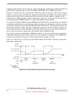
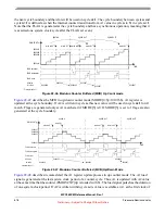
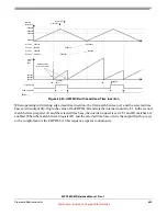
it is assumed that both the channel and global prescalers are set to $1 (each divide ratio is
two), meaning that the channel internal counter transitions at every four system clock cycles. FLAGs can
be generated only on B1 matches when MODE[5] is cleared, or on both A1 and B1 matches when
MODE[5] is set. Since B1 flag occurs at the cycle boundary, this flag can be used to indicate that A2 or
B2 data written on cycle
n
were loaded to A1 or B1, respectively, thus generating matches in cycle
n+1
.
Note that the FLAG has a synchronous operation, meaning that it is asserted one system clock cycle after
the FLAG set event.
1
4
match A1 negedge detection
5
A1 value
$000004
A1 match
A1 match negedge detection
output pin
EDPOL = 0
EMIOSCNT
TIME
match B1 negedge detection
B1 match
B1 match negedge detection
B1 value
$000008
system clock
prescaler
A2 value
$000000
write to A2
$000000
A1 match posedge detection
match A1 posedge detection
no transition at this point
1
cycle n
cycle n+1
Prescaler ratio = 2


