


MPC563XM Reference Manual, Rev. 1
682
Freescale Semiconductor
Preliminary—Subject to Change Without Notice
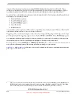
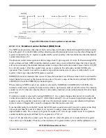
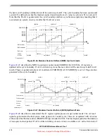
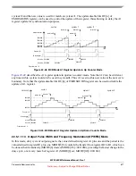
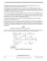
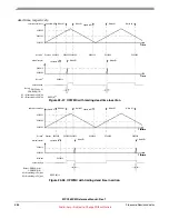
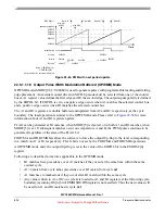
Figure 22-54. OPWFMB A1 and B1 Registers Update and Flags
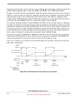
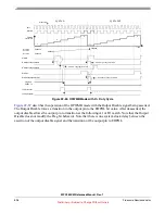
describes the operation of the Output Disable feature in OPWFMB mode. Differently from
the OPWFM mode, the output disable forces the channel output flip-flop to EDPOL bit value. This
functionality targets applications that use active high signals and a high to low transition at A1 match. In
this case EDPOL should be set to 0. Note that both the channel and global prescalers are set to $0 (each
divide ratio is one), meaning that the channel internal counter transitions at every system clock cycle.
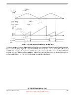
EDPOL = 0
cycle n
cycle n+1
cycle n+2
A1 value
1
B1 value
B2 value
$8
$2
$6
$8
$1
internal counter
$4
$6
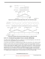
MODE
[6]
= 1
A2 value
1
$2
$4
$6
$2
$4
$6
$8
$6
Output pin
write to B2
write to A2
write to A2
Match A1
Match A1
Match B1
Match B1
Match B1
A1/B1 load signal
due to B1 match cycle n-1
FLAG set event
FLAG pin/register
Prescaler ratio = 4
FLAG clear


