


MPC563XM Reference Manual, Rev. 1
1154
Freescale Semiconductor
Preliminary—Subject to Change Without Notice
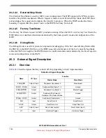
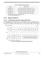
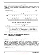
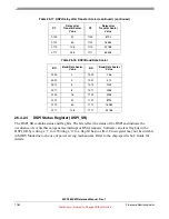
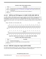
Table 26-4. DSPI_MCR Field Descriptions
Field
Description
0
MSTR
Master/Slave Mode Select. The MSTR bit configures the DSPI for either Master Mode or Slave Mode.
0 DSPI is in Slave Mode
1 DSPI is in Master Mode
1
CONT_SCK
E
Continuous SCK Enable. The CONT_SCKE bit enables the Serial Communication Clock (SCK) to
run continuously. See
Section 26.5.8, “Continuous Serial Communications Clock
,” for details.
0 Continuous SCK disabled
1 Continuous SCK enabled
2–3
DCONF[0:1]
DSPI Configuration. The DCONF field selects between the three different configurations of the DSPI.
The values below list the DCONF values for the various configurations.
4
FRZ
Freeze. The FRZ bit enables the DSPI transfers to be stopped on the next frame boundary when the
SoC enters Debug Mode.
0 Do not halt serial transfers1Halt serial transfers
5
MTFE
Modified Timing Format Enable. The MTFE bit enables a modified transfer format to be used. See
Section 26.5.7.4, “Modified SPI/DSI Transfer Format (MTFE = 1, CPHA = 1)
,” for more information.
0 Modified SPI transfer format disabled
1 Modified SPI transfer format enabled
6
PCSSE
Peripheral Chip Select Strobe Enable. The PCSSE bit enables the PCS[5]/PCSS to operate as an
PCS Strobe output signal. See
Section 26.5.6.5, “Peripheral Chip Select Strobe Enable (PCSS)
,” for
more information.
0 PCS[5]/PCSS is used as the Peripheral Chip Select[5] signal
1 PCS[5]/PCSS is used as an active-low PCS Strobe signal
7
ROOE
Receive FIFO Overflow Overwrite Enable. The ROOE bit enables an RX FIFO overflow condition to
either ignore the incoming serial data or to overwrite existing data. If the RX FIFO is full and new data
is received, the data from the transfer that generated the overflow is either ignored or shifted in to the
shift register. If the ROOE bit is asserted, the incoming data is shifted in to the shift register. If the
ROOE bit is negated, the incoming data is ignored. See
Section 26.5.10.6, “Receive FIFO Overflow
,” for more information.
0 Incoming data is ignored
1 Incoming data is shifted in to the shift register
8–15
PCSIS
x
Peripheral Chip Select Inactive State. The PCSIS bit determines the inactive state of the PCS
x
signal.
0 The inactive state of PCS
x
is low
1 The inactive state of PCS
x
is high
16
DOZE
Doze Enable. The DOZE bit provides support for externally controlled Doze Mode power-saving
mechanism. See
Section 26.5.11, “Power Saving Features
,” for details.
Table 26-5.
DCONF
DSPI Configuration
00
SPI
01
DSI
10
CSI
11
R
d


