


MPC563XM Reference Manual, Rev. 1
Freescale Semiconductor
1223
Preliminary—Subject to Change Without Notice
27.3.2.7
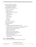
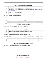
SCI Data Register High (SCIDRH)
This register is used to provide transmit data and retrieve received data in SCI mode. In LIN mode any
write access to this register is ignored and any read access returns all 0. In case of data transmission this
register is used to provide a part of the transmit data. In case of data reception this register provides a part
of the received data and related error information.
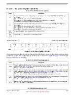
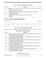
Table 27-11. SCICR4 Field Descriptions
Field
Description
7
BESM
Fast Bit Error Detection Sample Mode. This bit defines the sample point for the Fast Bit Error Detection Mode.
0 Sample point is RS9.
1 Sample point is RS13.
Note:
This bit is used in LIN mode only.
6
BESTP
Bit Error Stop. Stops the SCI when a Bit Error is asserted. This allows to stop driving the LIN bus quickly after a
Bit Error has been detected. The SCI won’t start a new byte transmission until the time for the current byte has
expired.
0 Transmission is not stopped on bit error.
1 Transmission is stopped on bit error.
Note:
This bit is used in LIN mode only.
5
RXPOL
RXD Pin polarity. This bit controls the polarity of the RXD pin. See
Section 27.4.2.1.1, “Inverted Data Frame
0 Normal Polarity.
1 Inverted Polarity.
4
PMSK
Parity Bit Masking. This bit defines whether the received parity bit is presented in the related bit position in the
SCI Data Register High (SCIDRH)
or
SCI Data Register Low (SCIDRL)
0 The received parity bit is presented in the bit position related to the parity bit.
1 The value 0 is presented in the bit position related to the parity bit.
3
ORIE
Overrun Interrupt Enable. This bit controls the SCISR1[OR] interrupt request generation.
0 OR interrupt request generation disabled.
1 OR interrupt request generation enabled.
2
NFIE
Noise Interrupt Enable. This bit controls the SCISR1[NF] interrupt request generation.
0 NF interrupt request generation disabled.
1 NF interrupt request generation enabled.
1
FEIE
Frame Error Interrupt Enable. This bit controls the SCISR1[FE] interrupt request generation.
0 FE interrupt request generation disabled.
1 FE interrupt request generation enabled.
0
PFIE
Parity Error Interrupt Enable. This bit controls the SCISR1[PF] interrupt request generation.
0 PF interrupt request generation disabled.
1 PF interrupt request generation enabled.
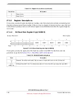
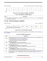
Address Offset: 0x06
Access: User read/write
7
6
5
4
3
2
1
0
R
RN
TN
ERR
0
R[11:8]
W
Reset
0
0
0
0
0
0
0
0
Figure 27-8. SCI Data Register High (SCIDRH)


