


MPC563XM Reference Manual, Rev. 1
Freescale Semiconductor
383
Preliminary—Subject to Change Without Notice
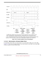
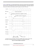
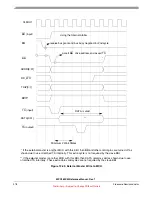
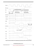
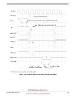
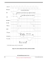
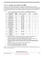
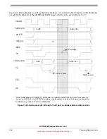
Figure 13-46. External Master Read followed by MCU Read to Same CS Bank
CLKOUT
ADDR[3:31]
TS
RD_WR
TSIZ[0:1]
DATA[0:31]
TA
DATA is valid
BR (input)
BG
BB
receive bus grant and bus busy negated for 2nd cycle
Ext. master starts
Using the Internal arbiter
BDIP
read access
MCU starts
read access
DATA is valid
OE
CSx
Both masters off
Ext. master and MCU off


